


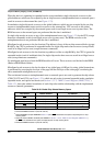
Chapter 23 Memory Mapping Control (S12XMMCV2)
MC9S12XDP512 Data Sheet, Rev. 2.11
904 Freescale Semiconductor
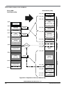
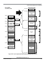
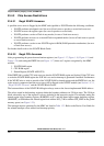
When the device is operating in expanded modes except emulation single-chip mode, accesses to the
global addresses which are not occupied by the on-chip resources (unimplemented areas or external space)
result in accesses to the external bus (see Figure 1-23).
In emulation single-chip mode, accesses to the global addresses which are not occupied by the on-chip
resources (unimplemented areas) result in accesses to the external bus. CPU accesses to the global
addresses which are occupied by the external space result in an illegal access reset (system reset). The
BDM accesses to the external space are performed but the data is undefined.
In single-chip modes an access to any of the unimplemented areas (see Figure 1-23) by the CPU (except
firmware commands) results in an illegal access reset (system reset). The BDM accesses to the
unimplemented areas are performed but the data is undefined.
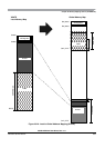
Misaligned word accesses to the last location (Top address) of any of the on-chip resource blocks (except
RAM) by the CPU is performed in expanded modes. In single-chip modes these accesses (except Flash)
result in an illegal access reset (except firmware commands).
Misaligned word accesses to the last location (top address) of the on-chip RAM by the CPU is ignored in
expanded modes (read of undefined data). In single-chip modes these accesses result in an illegal access
reset (except firmware commands).
No misaligned word access from the BDM module will occur. These accesses are blocked in the BDM
(Refer to BDM Block Guide).
Misaligned word accesses to the last location of any global page (64 Kbyte) by using global instructions,
is performed by accessing the last byte of the page and the first byte of the same page, considering the
above mentioned misaligned access cases.
The non internal resources (unimplemented areas or external space) are used to generate the chip selects
(CS0,CS1,CS2 and CS3) (see Figure 1-23), which are only active in normal expanded mode, emulation
expanded mode, and special test mode (see Section 1.3.2.1, “MMC Control Register (MMCCTL0)”).
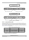
Table 1-21 shows the address boundaries of each chip select and the relationship with the implemented
resources (internal) parameters.
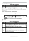
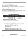
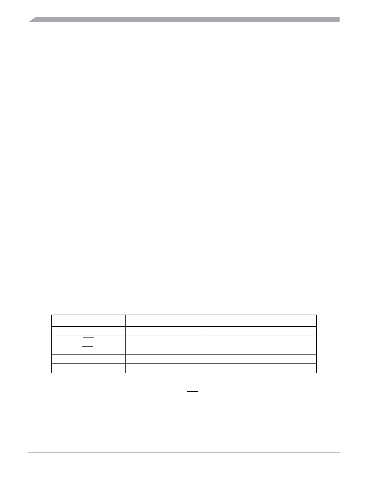
Table 23-20. Global Chip Selects Memory Space
Chip Selects Bottom Address Top Address
CS3 $00_0800 $0F_FFFF minus RAMSIZE
1
1
External RPAGE accesses in (NX, EX and ST)
CS2 $10_0000 $13_FFFF minus EEPROMSIZE
2
2
External EPAGE accesses in (NX, EX and ST)
CS2
3
3
When ROMHMis set (see ROMHM in Table 1-19) the CS2 is asserted in the space occupied by this on-chip
memory block.
$14_0000 $1F_FFFF
CS1 $20_0000 $3F_FFFF
CS0
4
4
When the internal NVM is enabled (see ROMON in Section 1.3.2.5, “MMC Control Register (MMCCTL1)”)
the
CS0 is not asserted in the space occupied by this on-chip memory block.
$40_0000 $7F_FFFF minus FLASHSIZE
5
5
External PPAGE accesses in (NX, EX and ST)