


Chapter 20 Debug (S12XDBGV2)
MC9S12XDP512 Data Sheet, Rev. 2.11
804 Freescale Semiconductor
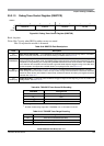
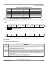
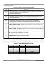
20.3.1.9 Debug State Control Register 2 (DBGSCR2)
Read: Anytime
Write: Anytime when DBG not armed.
This register is visible at 0x0027 only with COMRV[1:0] = 01. The state control register 2 selects the
targeted next state while in State2. The matches refer to the match channels of the comparator match
control logic as depicted in Figure 20-1 and described in Section 20.3.1.11.1, “Debug Comparator Control
Register (DBGXCTL)”. Comparators must be enabled by setting the comparator enable bit in the
associated DBGXCTL control register.
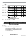
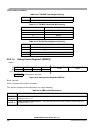
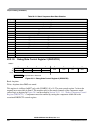
Table 20-21. State1 Sequencer Next Sate Selection
SC[3:0] Description
0000 Any match triggers to state2
0001 Any match triggers to state3
0010 Any match triggers to final state
0011 Match2 triggers to State2....... Other matches have no effect
0100 Match2 triggers to State3....... Other matches have no effect
0101 Match2 triggers to final state....... Other matches have no effect
0110 Match0 triggers to State2....... Match1 triggers to State3....... Other matches have no effect
0111 Match1 triggers to State3....... Match0 triggers final state....... Other matches have no effect
1000 Match0 triggers to State2....... Match2 triggers to State3....... Other matches have no effect
1001 Match2 triggers to State3....... Match0 triggers final state....... Other matches have no effect
1010 Match1 triggers to State2....... Match3 triggers to State3....... Other matches have no effect
1011 Match3 triggers to State3....... Match1 triggers to final state....... Other matches have no effect
1100 Reserved
1101 Reserved
1110 Reserved
1111 Reserved
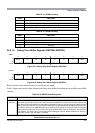
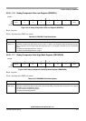
0x0027
76543210
R0000
SC3 SC2 SC1 SC0
W
Reset 00000000
Unimplemented or Reserved
Figure 20-11. Debug State Control Register 2 (DBGSCR2)