


Chapter 4 Port Integration Module (S12XDP512PIMV2)
MC9S12XDP512 Data Sheet, Rev. 2.11
244 Freescale Semiconductor
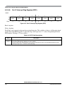
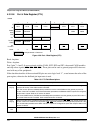
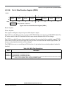
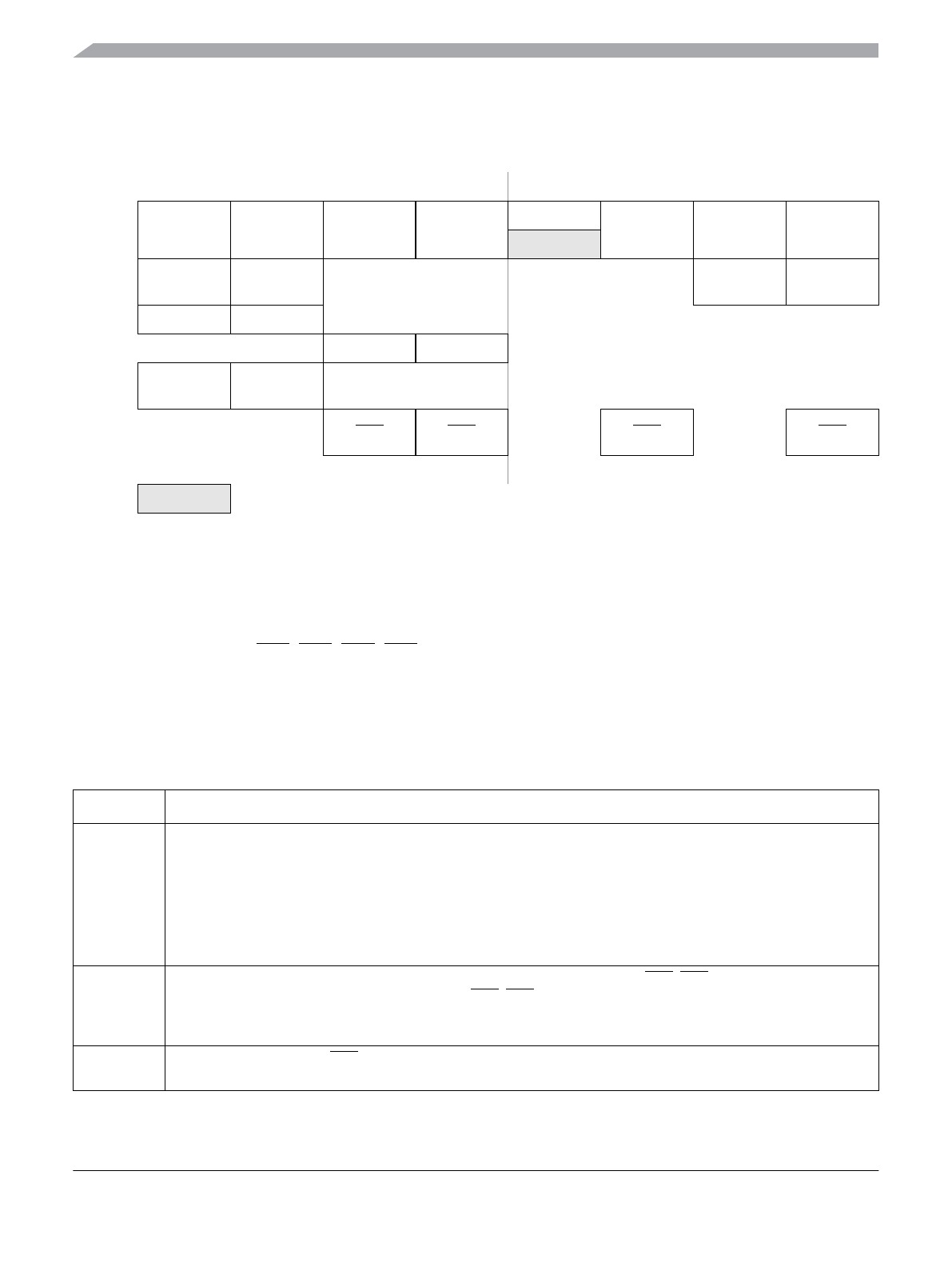
4.3.2.54 Port J Data Register (PTJ)
Read: Anytime.
Write: Anytime.
Port J pins 7–4 and 2–0 are associated with the CAN4, SCI2, IIC0 and IIC1, the routed CAN0 modules
and chip select signals (
CS0, CS1, CS2, CS3). These pins can be used as general purpose I/O when not
used with any of the peripherals.
If the data direction bits of the associated I/O pins are set to logic level “1”, a read returns the value of the
port register, otherwise the buffered pin input state is read.
0x0268
76543210
R
PTJ7 PTJ6 PTJ5 PTJ4
0
PTJ2 PTJ1 PTJ0
W
CAN4/
SCI2
TXCAN4 RXCAN4 TXD2 RXD2
IICO SCL0 SDA0
IIC1 SCL1 SDA1
Routed
CAN0
TXCAN0 RXCAN0
Alt.
Function
CS2 CS0 CS1 CS3
Reset 00000000
= Unimplemented or Reserved
Figure 4-56. Port J Data Register (PTJ)
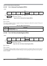
Table 4-51. PTJ Field Descriptions
Field Description
7–6
PJ[7:0]
The CAN4 function (TXCAN4 and RXCAN4) takes precedence over the IIC0, the routed CAN0 and the general
purpose I/O function if the CAN4 module is enabled.
The IIC0 function (SCL0 and SDA0) takes precedence over the routed CAN0 and the general purpose I/O
function if the IIC0 is enabled. If the IIC0 module takes precedence the SDA0 and SCL0 outputs are configured
as open drain outputs. Refer to IIC section for details.
The routed CAN0 function (TXCAN0 and RXCAN0) takes precedence over the general purpose I/O function if
the routed CAN0 module is enabled. Refer to MSCAN section for details.
5-4
PJ[5:4]
The IIC1 function (SCL1 and SDA1) takes precedence over the chip select (CS0, CS2) and general purpose I/O
function if the IIC1 is enabled. The chip selects (
CS0, CS2) take precedence over the general purpose I/O. If the
IIC1 module takes precedence the SDA1 and SCL1 outputs are configured as open drain outputs. Refer to IIC
section for details.
2
PJ2
The chip select function (
CS1) takes precedence over the general purpose I/O.