


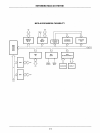


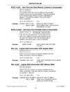
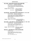
INSTRUCTION
SE;T
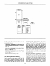
memory
banks.
The operation of the program
memory bank switch
is
explained
in
section
3.1.2.
The
working register bank switch
instructions
allow the programmer to imme-
diately substitute a second 8 register working
register bank for the one
in
use.
This
effectively provides
16
working registers
or
it
can
be
used
as
a means
of
quickly saving the
contents of the registers
in
response to
an
interrupt. The user has the option to switch
or
not to switch banks on interrupt. However, if
the banks
are
switched, the original bank will
be
automatically restored upon execution
of
a return and restore status instruction at the
end of
the.
interrupt service routine.
A special instruction enables
an
internal
clock, which
is
the XTAL frequency divided
by three, to be output on pin
TO.
This clock
can
be
used
as
a general purpose clock
in
the
users system. This instruction should
be
used only to initialize the system since the
clock output
can
be
disabled only by
application of system reset.
Input/Output
Instructions
Ports 1 and 2
are
8-bit static I/O ports which
can
be
loaded to and from the accumulator.
Outputs
are
statically latched but inputs are
not latched and must be
read
while inputs are
present.
In
addition, immediate data from
program memory
can
be
ANDed or
ORed
directly to Port 1 and Port 2 with the result
remaining
on
the port. This allows "masks"
stored
in
program memory to selectively set
or
reset individual bits
of
the I/O ports. Ports 1
and 2
are
configured to allow input on a given
pin by first writing a "1" out to the pin.
An 8-bit port
called BUS can also
be
accessed via the accumulator and
can
have
statically latched outputs
as
well. It too can
have immediate data ANDed or
ORed
directly to its outputs, however, unlike ports 1
and
2,
all eight lines of BUS must
be
treated
as
either input
or
output at
anyone
time.
In
addition to being a static port, BUS
can
be
used
as
a true synchronous bi-directional
port using the Move External instructions
used to access external data memory. When
these instructions are executed a cor-
4·4
responding READ
or
WRITE pulse is
generated and data is valid only at that time.
When data
is
not being transferred BUS is in
a high impedance state.
The basic three on board
I/O ports can
be
expanded via a 4-bit expander bus using half
of
port
2.
I/O expander devices on this bus
consist of four 4-bit ports which are
addressed
as
ports 4 through
7.
These ports
have their own AND and
OR
instructions like
the on board ports
as
well
as
move
instructions to transfer data in or out. The
expander AND and
OR
instructions, how-
ever,
combine the contents of accumu-
lator with the selected port rather than
immediate data
as
is
done with the
on
board
ports.
I/O devices can also
be
added externally
using the BUS port
as
the expansion
bus.
In
this case the I/O ports become "memory
mapped",
i.e.
they are addressed
in
the same
way
as
external data memory and exist in the
external data memory address space ad-
dressed by pointer register
RO
or
R1.
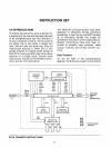
4.1
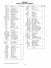
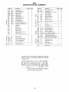
Instruction Set Description
The following pages describe the MCS-48
instruction set in detail. The instruction set is
first summarized with instructions grouped
functionally. This summary page
is
followed
by a detailed description listed alphabetically
by mnemonic opcode.
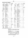
The alphabetical listing includes the
follow-
ing information:
Mnemonic
Machine Code
Verbal Description
Symbolic Description
Assembly Language Example
The machine code
is
represented with the
most significant bit
(7)
to the left and two byte
instructions
are
represented with the first
byte on the left. The assembly language
examples are formulated
as
follows:
Arbitrary
Label:
Mnemonic,
Operand;
Descriptive
Comment
See
section
1.2.2
for a description and
example of
an
assembly language program.