


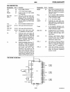
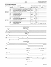
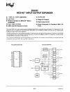
PIN DESCRIPTION
Symbol
PROG
P20-P23
GND
P40-P43
P50-P53
P60-P63
P70-P73
Vee
Pin No. Function
7 Clock
Input. A high to low
transistion on PROG signi.fies
that address and control are
available on P20-P23, and a low
to high transition signifies that
data is available on P20-23.
6
Chip Select Input. A high on CS
inhil;lits any change
of
output
or
internal status.
11-8 Four (4) bit bi-directional
port
contains the address and con-
trol bits on a high
to'
low
transition
of
PROG. During a
low to high transition contains
the data
for
a selected
output
port
if
a write operation,
or
the
data from a selected port before
the
low
to
high transition
if
a
read operation.
12
2-5
1,23-21
20-17
13-16
o volt supply.
Four (4)
bit
bi-directional
110
ports. May
be
programmed
to
be
input
(during read),
low
impedance latched
output
(after write)
or
a tri-state (after
read). Data on pins
P20-23 may
be directly written, ANDed
or
ORed with previous data.
24
+5
volt supply.
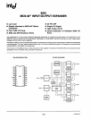
FUNCTIONAL DESCRIPTION
General Operation
The 8243 contains
four
4-bit
1/0
ports which serve
as
an
extension
of
the on-chip
1/0
and are addressed
as
ports
4-
7.
The following operations may be performed on these
ports:
• Transfer Accumulator to Port.
• Transfer Port to Accumulator.
• AND Accumulator
to
Port,
•
OR
Accumulator to Port.
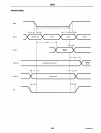
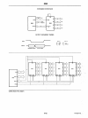
All communication between the 8048 and the 8243 occurs
over Port 2 (P20-P23) with timing provided by
an
output
pulse on the PROG
pi'n
of
the processor. Each transfer
consists of
two
4-bit nibbles:
The first containing the
"op code" and port address and
the second containing the actual 4-bits
of
data.
8243
A high to
low
transition
of
the PROG line indicates that
address is present while a
low
to
high
transition indicates
the presence
of
data. Additional 8243's may
be
added to
the 4-bit bus and chip selected using additional
output
lines
from
the 8048/8748/8035.
Power On Initialization
Initial application
of
power
to
the device forces
input/output
ports
4,
5,
6,
and 7
to
the tri-state and port 2
to
the input mode. The PROG pin may be either:high
or
low
when power is applied. The first high to low transition
of
PROG causes device
to
exit power on mode. The power on
sequence is initiated
if
Vee
drops below
1V.
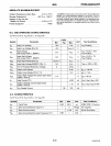
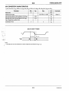
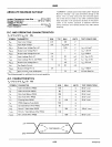
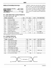
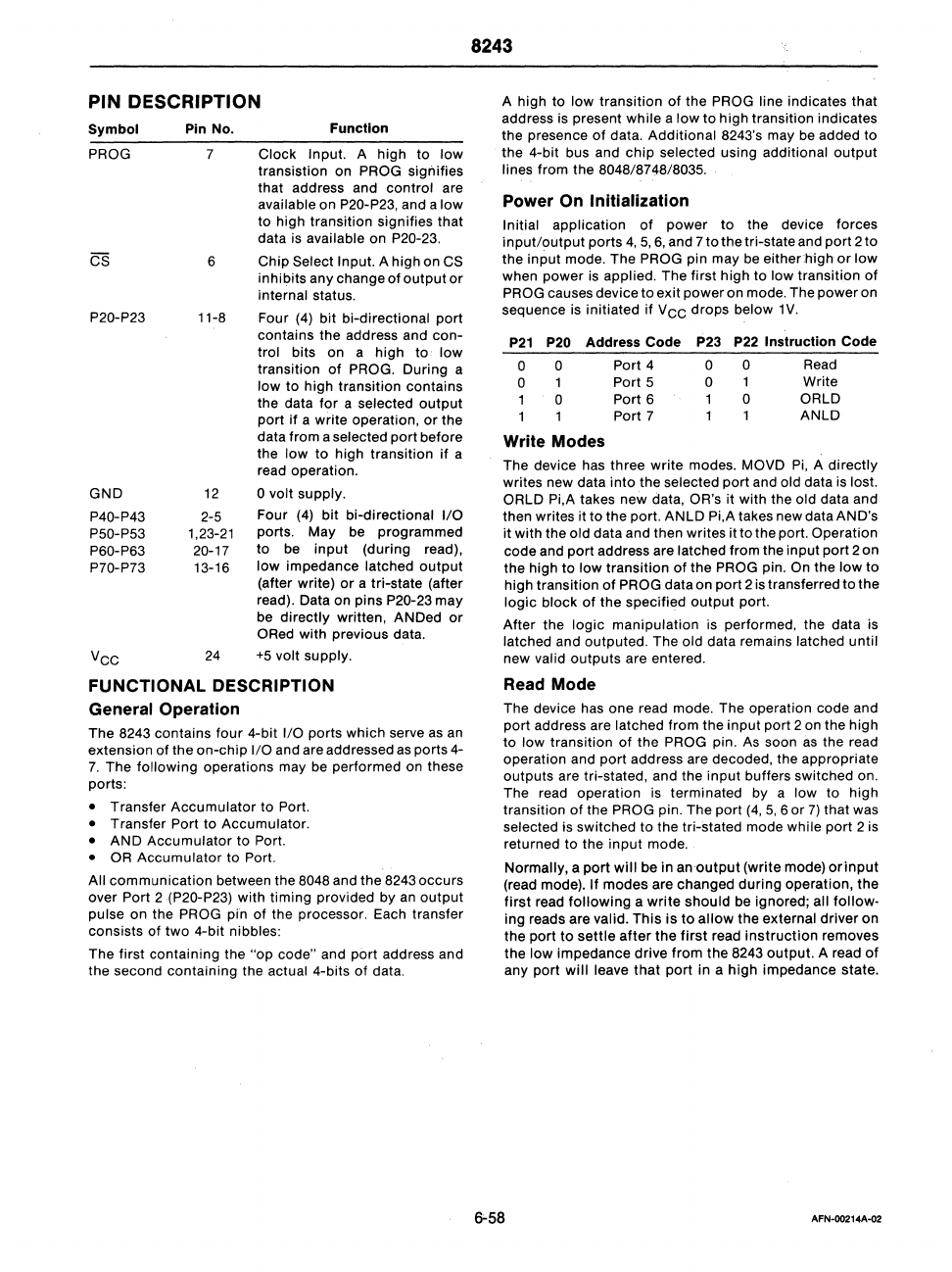
P21
P20
Address Code P23
P22
Instruction Code
0
0
Port 4 0
0
Read
0
1
Port 5
0
Write
1
0
Port 6 1
0
ORlD
1
Port 7
ANlD
Write Modes
The device has three write modes. MOVD
Pi,
A directly
writes new data
into
the selected port and old data is lost.
ORlD
Pi,A takes new data, OR's it with the old data and
then writes it to the port.
ANlD
Pi,A takes new data AND's
it
with the old data and then writes it to the port. Operation
code and port address are latched from the input port 2 on
the high to low transition
of
the PROG pin. On the
low
to
high transition
of
PROG data on port 2 is transferred
to
the
logic
block
of
the specified
output
port.
After the logic manipulation is performed, the data is
latched and outputed. The old data remains latched until
new valid outputs are entered.
Read Mode
The device
has
one read mode. The operation code and
port address are latched from the input port 2 on the high
to
low
transition
of
the PROG pin. As soon
as
the read
operation and port address are decoded, the appropriate
outputs are tri-stated, and the input buffers switched on.
The read operation is terminated by a low to high
transition
of
the PROG pin. The port
(4,
5,
6
or
7)
that was
selected Is switched
to
the tri-stated mode while port 2 is
returned to the
input
mode.
Normally, a port
will
be in
an'output
(write mode)
orinput
(read mode).
If
modes are changed during operation,
the
first
read
following
a
write
should be ignored; all follow-
ing reads are valid.
This
is
to
allow
the external driver on
the port
to
settle
after
the
first
read
instruction
removes
the
low
impedance drive from the 8243 output. A read
of
any port
will
leave
that
port in a
high
impedance state.
&-58
AFN-00214A-Q2