


SINGLE
COMPONENT
SYSTEM
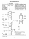
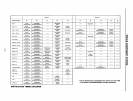
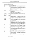
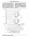
Pin*
Designation Number Function
Vss
Voo
Vee
PROG
P10-P17
(Port
1)
P20-P27
(Port
2)
00-07
(BUS)
TO
T1
20
Circuit
GND
potential
26
Programming power supply; + 25V during program,
+
5V
during operation for both
ROM
and
PROM.
low
power standby pin
in
8048
ROM
version
40
Main power supply; + 5V during operation and
8748
programming.
25
Program pulse
(+23V)
input pin during 8748
programming.
Output strobe for 8243
I/O expander.
27-34 8-bit quasi-bidirectional port.
(Internal Pullup
""
50KOJ
21-24 8-bit quasi-bidirectional port. (Internal Pullup
""
50KOJ
35-38
P20-P23 contain the four high order program counter
bits during
an
external program memory fetch and serve
as
a 4-bit I/O expander bus for
8243.
12-19
True
bidirectional port which can
be
written or read syn-
chronously using the
RO,
WR
strobes. The port can also
be
statically latched.
1
39
6
8
Contains the 8 low order program counter bits during
an
external program memory fetch,
and
receives the ad-
dressed instruction under the
control of
PSEN.
Also con"
tains the address
and
data during
an
external
RAM
data
store instruction, under
control of
ALE,
RD,
and
WR.
Input pin testable using the conditional transfer instruc-
tions
JTO
and
JNTO.
TO
can
be
designated
as
a clock
output using
ENTO
ClK
instruction.
TO
is
also used dur-
ing programming.
Input
pin
testable using the
JT1,
and
JNT1
instructions.
Can
be
designated the event counter input using
the
STRT CNT instruction.
Interrupt input. Initiates
an
interrupt if interrupt
is
enabled.
Interrupt
is
disabled after a reset. (Active low)
Output strobe activated during a
BUS
read. Can
be
used to enable data onto the
BUS
from
an
external
device. (Active low)
Used
as
a
Read
Strobe to External Data Memory.
*8048,8748,8049
2·15