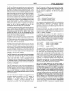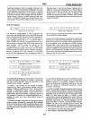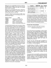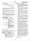
The BO and
BI
interrupts enable the user
to
perform data
transfer
cycles. BO indicates that a byte has been sent
to
the GPIB
or
the 8291 has been addressed
to
talk. A new
data byte may be written
into
the Data Out register. It is set
by the occurrence
of
TACS.
(SWNS + SGNS). Hence, it
is
reset when a data byte is written
into
the Data
Out
register,
when ATN
is
asserted on the GPIB, or when the device
stops being addressed to
talk. Similarly,
BI
is set when
an
input
byte is accepted into the 8291 and reset when the
microprocessor reads the Data
In register. BO and
BI
are
also reset by pon (power-on local message) and by a read
of
the Interrupt Status 1 register. However, if it is so
desired, data transfer
cycles may
be
performed
without
reading the Interrupt Status 1 register if all interrupts
except for
80
or
BI
are enabled;
BO
and
BI
will
automatically
reset after each byte is transferred.
If
the
8291 is used
without
DMA, the
BO
and
BI
interrupts
may be
enabled through the DREQ pin. The DMAO and
DMAI bits in the Interrupt Enable 2 register would be the
corresponding
enable
bits
for
this feature. Thus, imple-
menting this feature,
with
80
and
Bi
enabied
from
the
INT pin, allows for servicing
of
these interrupts
without
reading the Interrupt Status registers.
8291
The
ERR
bit
is
set to indicate the bus error condition where
the
8291
is
an
active talker, tries sending a byte
to
the
GPIB, but there are no active listeners (e.g., all devices on
the
GPIB are in AIDS). The logical equivalent
of
(nba •
TACS •
DAC • RFD) will set this bit.
The DEC bit
is
set whenever DCAS has occurred. The user
must define a known state to which
all device functions
will return in DCAS.
Typically
this state will be a power-on
state. However, the state of the device functions at
DCAS
is
at the designer's discretion. It should be noted that
DCAS has no effect on the interface functions which are
returned
to
a known state by the IFC (interface clear)
message
or
the pon local message.
The END
Interrupt
bit
may be used by the microprocessor
to
detect that a mUlti-byte transfer has been completed.
The bit
will be set when the 8291
is
an
active listener
(LACS)
and either EOS or
EOI
is
received. EOS will
generate
an
interrupt
when the byte in the Data In regis-
ter
matches
the
byte in the
EOS
register. Otherwise the
interrupt
will be generated when a true
input
is
detected at
the
EOI pin
of
the 8291.
The GET interrupt bit
is
used by the microprocessor to
detect that
DTAS has occurred. It
is
set by the 8291 when
the
GET message is received
while
it
is
addressed
to
lis-
ten. The TRIG
output
pin
of
the
8291 is
also
asserted
when the GET message is received. Thus,
the
basic
operation
of
the
device may be started
without
involving
the
microprocessor.
The APT interrupt bit indicates
to
the processor that a
secondary address
is
available in the CPT register for
validation. This interrupt
will only
occur
if Mode 3
addressing
is
in effect. (Refer
to
the section on
addressing.)
In Mode
2,
secondary addresses will
be
recognized on the 8291. They will be ignored in Mode 1.
The CPT interrupt bit flags
the
occurrence
of
an unde-
fined command and
of
all secondary commands follow-
ing
an
undefined command. The Command pass
through
feature is enabled by
the
BO
bit
of
Auxiliary
register
B.
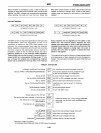
UDC = [UCG + ACG(TADSoPPC
+ LADSoTCT)]oundefinedoBO
where:
ACG - Addressed Command
Group
UCG - Universal Command
Group
SCG - Secondary Command
Group
Any
message not decoded by the 8291 (not included in the
state diagrams in Appendix
B)
becomes
an
undefined
command. Note from the
logic equation that any
addressed command
is
automatically ignored when the
8291 is not addressed.
Undefined commands are read by the CPU from the
Command Pass
Through
Register
of
the 8291. Until this
register
is
read, the 8291 will hold off the handshake (only
ii
the
CP
I teatu
re
is
enabled).
An especially useful feature
of
the 8291
is
its ability
to
generate interrupts from state transitions in the interface
functions.
In particular, the lower 4 bits
of
the Interrupt
Status 2 register, if enabled by the corresponding enable
bits, will cause
an
interrupt upon changes in the follow-
ing states as defined in IEEE 488:
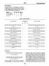
Bit 0 ADSC
Bit 1 RLC
Bit 2
LLOC
Bit 3 SPASC
change in LIDS
or
TIDS
or
MJMN
change in
LOCS or REMS
change in LWLS
or
RWLS
change in SPAS
The upper 4 bits
of
the I nterrupt Status 2 register are
available
to
the processor
as
status bits. Thus,
if
one of the
bits 1-3 generates
an
interrupt indicating a state change
has taken
place, the corresponding status bit (bits 5-7)
may be read to determine what
the
new state
is.
To
determine the nature
of
a change in addressed status (bit
0)
the Address Status Register
is
available to be read. And
finally, bit 7 monitors the state
of
the 8291 INT pin.
Logically,
it
is
an
OR
of
all enabled
interrupt
status
bits.
One
should
note
that
bits
4-7
of
the Interrupt Status 2
Register
do
not
generate interrupts, but are available
only
to
be read as
status
bits
by
the
processor.
Bits
4 and 5 (DMAI, DMAO)
of
the Interrupt Enable 2
Register are
available
to
enable
direct
data transfers
between memory and the
GPIB, DMAI (DMA in) enables
the DREQ (DMA request) pin
of
the 8291
to
be asserted
upon the occurrence
of
81.
Similarly, DMAO (DMA out)
enables the
DREQ
pin
to
be
asserted upon the occurrence
of
BO. One
might
note that
the
DREQ pin may be used as
a second interrupt
output
pin, monitoring
BI
and/or
BO
and enabled
by
DMAI and DMAO. One should note that
the
DREQ
pin is not affected by a read
of
the Interrupt
Status 1 Register. It is reset whenever a byte is written
to
the Data Out Register
or
read from
the
Data In Register.
To
ensure that an interrupt status bit will
not
be cleared
without
being read, and will
not
remain uncleared after
being read, the
8291
Irnplem~Jnts
a special Interrupt
9-90


