


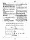
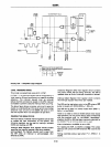
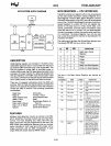
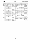
8272
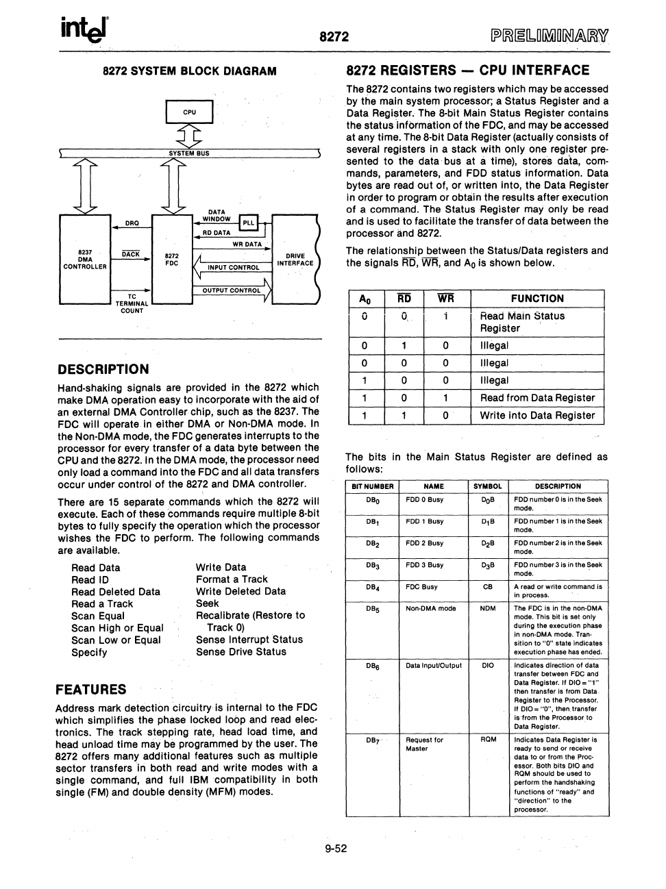
8272 SYSTEM BLOCK DIAGRAM
8237
i5ACK
DMA
CONTROLLER
TC
8272
FDC
L-
__
--I
TERMINAL
L....
__
.J
COUNT
DESCRIPTION
Hand-shaking signals are provided in the
8272
which
make DMA operation easy to incorporate with the aid
of
an external DMA Controller chip, such
as
the
8237.
The
FDC
will
operate in either DMA or Non-DMA mode.
In
the Non-DMA mode, the FDC generates interrupts
to
the
processor for every transfer
of
a data byte between the
CPU
and the
8272.
In
the DMA mode, the processor need
only load a command into the
FDC
and
all data transfers
occur under
control
of
the
8272
and DMA controller.
There are
15
separate commands which the
8272
will
execute.
Each
of
these commands require multiple 8-bit
bytes to
fully specify the operation which the processor
wishes the
FDC to perform. The following commands
are available.
Read
Data
Read
ID
Read
Deleted Data
Read
a Track
Scan Equal
Scan High
or
Equal
Scan Low or Equal
Specify
FEATURES
Write Data
Format a Track
Write Deleted Data
Seek
Recalibrate (Restore
to
Track
0)
Sense Interrupt Status
Sense Drive Status
Address mark detection circuitry is internal to the
FDC
which simplifies the phase locked loop and
read
elec-
tronics. The track stepping rate, head load time, and
head unload time may be programmed by the user. The
8272 offers many additional features such
as
multiple
sector transfers in both
read
and write modes with a
single command, and
full IBM compatibility in both
single (FM) and double density (MFM) modes.
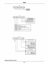
8272 REGISTERS
CPU INTERFACE
The
8272
contains two registers which may
be
accessed
by the main system processor; a Status Register and a
Data
Register, The 8-bit Main Status Register contains
the status information of the
FDC,
and may
be
accessed
at any time.
The
8-bit Data Register (actually consists of
several registers in a stack with only one register
pre-
sented
to
the data· bus at a time), stores data, com-
mands, parameters, and
FDD
status information. Data
bytes are
read
out of, or written into, the Data Register
in order to program or obtain the results after execution
of
a command. The Status Register may only be read
and is used to facilitate the transfer
of
data between the
processor
and
8272.
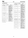
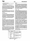
The relationship between the Status/Data registers
and
the signals
RD,
WR,
and
Ao
is shown below.
Ao
RD
WR
FUNCTION
0
0
i
Head
Main l::itatus
Register
0
1 0
Illegal
0 0 0
Illegal
1 0 0
Illegal
1 0 1
Read
from Data Register
1
1
0
Write into Data Register
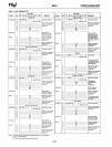
The bits in the Main Status Register are defined
as
follows:
BIT NUMBER
NAME SYMBOL DESCRIPTION
08
0
FOO
0 Busy
00
8
FOO
numberO is in
the
Seek
mode.
08,
FDD 1
Busy
0,8
FOO
number
1
is
in the Seek
mode.
08
2
FDD 2 Busy
02
8
FOD
number2
is
in
the
Seek
mode.
08
3
FOD
3 Busy
03
8
FDO
number3
is
in
the
Seek
mode.
08
4
FOC
Busy
C8
A read
or
write command
is
in process.
08
5
Non·DMA mode
NOM
The
FOe
is
in
the
non·DMA
mode.
This
bit
is
set
only
during
the
execution phase
in
non·DMA
mode. Tran-
sition
to
"0"
state indicates
execution
phase has ended.
08
6
Data
Input/Output
010
Indicates
direction
of
data
transfer
between
FOe
and
Data Register.
If
010="1"
then
transfer
Is from Data
Register
to
the Processor.
If
010
=
"0",
then_
transfer
is
-from the Processor
to
Data Register.
08
7
Request
for
ROM
Indicates
Data Register is
Master
ready
to
send
or
receive
data
to
or
from
the
Proc·
essor. Both
bits
010 and
ROM
should
be used to
perform
the
handshaking
functions
of
"ready"
and
"direction"
to
the
processor.
9-52