8205
APPLICATIONS
OF
THE 8205
The 8206 can be used
in
a wide variety of applications in
microcomputer systems.
I/O ports can be decoded from
the
address bus, chip select signals can
be
generated
to
select
memory devices and
the
type of machine state such
as
in
8008 systems can
~
derived from a simple decoding
of
the
state lines
(SO,
S1, S2) of
the
8008
CPU.
1/0
Port
Decoder
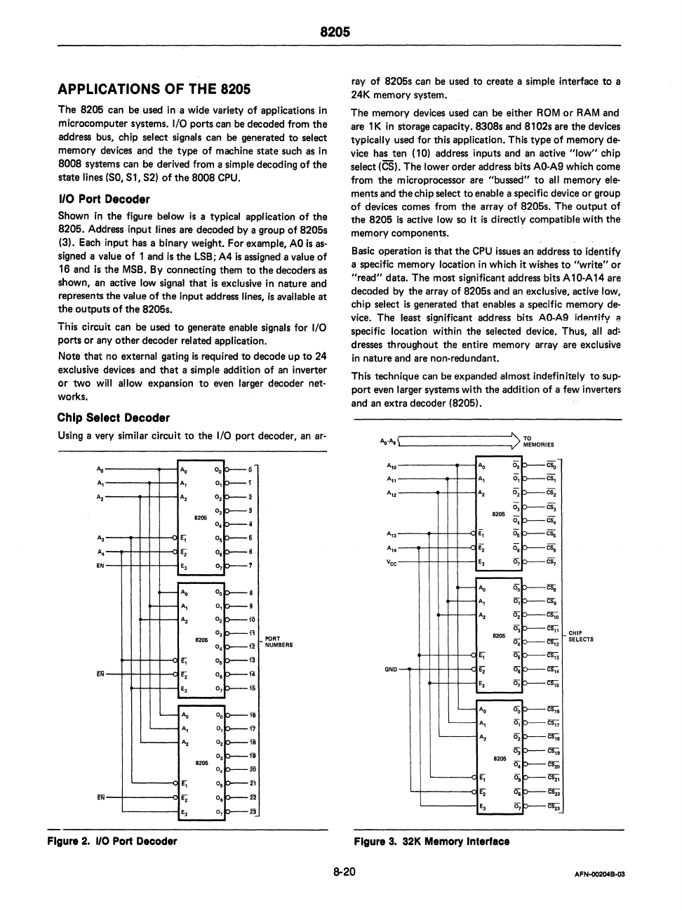
Shown
in
the
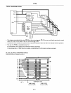
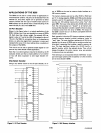
figure below
is
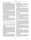
a typical application
of
the
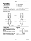
8206. Address input lines are decoded
by
a group of 8206s
(3).
Each
input has a binary weight. For example,
AO
is
as·
signed a value of 1 and
is
the
LSB;
A4
is
assigned a value of
16
and
is:
the
MSB.
By
connecting them to
the
decoders
as
shown,
an
active
low
signal that
is
exclusive in nature and
represents the value of
the
input address lines,
is
available
at
the outputs of
the
8206s.
This circuit can be used
to
generate enable signals for I/O
ports or any other decoder related application.
Note that
no
external gating
is
required
to
decode up
to
24
exclusive devices and
that
a simple addition of
an
inverter
or two
will
allow expansion
to
even larger decoder net·
works.
Chip
Select
Decoder
Using
a very similar circuit
to
the I/O port decoder,
an
ar·
"---~-I
A,---..,-r--t
A,,--~-+-+--t
A,
-T"1-t--t-1t--ClI
'N
-+-t-t--t-t---t
Eii-+-IH-+t-<:t
Figure
2.
1/0
Port
Decoder
A,
A,
A,
E1
..
'3
A.
A,
A,
E1
r,
'3
..
A,
A,
E1
r,
'3
8205
ili
f1
8205
PORT
12
NUMBERS
f3
~
i5
is
fi
is
11
8206
2ij
Ii
22
23
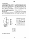
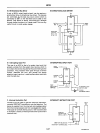
ray of 8205s can be used to create Ii simple interface
to
a
24K memory system.
The memory devices used can
be
either
ROM
or
RAM
and
are 1 K
in
storage capacity. 8308s and 81 02s are the devices
typically used for this application. This type of memory
de-
vice has ten (10) address inputs and
an
active
"low"
chip
select
(CS). The lower order address bits
AO·A9
which come
from
the
microprocessor are "bussed"
to
all
memory
ele-
ments
and
the
chip select
to
enable a specific device
or
group
of devices comes from the array
of
~206s.
The
output
of
the
8206
is
active low
so
it
is
directly compatible with
the
memory components.
Basic
operation
is
that
the
CPU
issues an address
to
identify
a specific memory location
in
which it wishes
to
"write" or
"read" data. The most significant address bits A 10·A 14 are
decoded by the array of 8206s and
an
exclusive, active low,
chip select
is
generated that enables a specific memory de·
vice. The least significant address bits
AO.A9
irt.!I1tify
!!
specific location within the selected device. Thus,
all
ad'
dresses th roughout the entire memory array are exclusive
in
nature and are non·redundant.
This technique can be expanded almost indefinitely
to
sup·
port even larger systems with the addition of a few inverters
and
an
extra decoder (8205).
.....
,1..
_______
_
A",----~_I
...
,---~+-I
A,,---.-1--+--1
A
13
--..,-H+-q
A
14
-_-t-H-+-q
Vee
--+--+-H-+--1
ONO
~>-+-t--Ht-t-q
..
A,
A,
E,
E,
'3
..
A,
A,
E,
E,
"
A,
A,
A,
E,
E,
'3
8206
8206
8206
Figure
3.
32K
Memory
Interface
>
~~MORIES
OS;
CIj
CIj
OS;;
cr,;
CHIP
es;;
SELECTS
es;;
Cfi4
OS;;
!!Iii
an
CI1a
es;;
ill;;;
~
csu
CliO
8-20
AFN-0020411-03


