


intel"
S04SH/S04SH-1/S035HL/S035HL-1
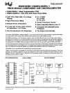
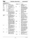
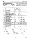
~!ru~[!"o!MlOOO~OOW
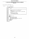
PIN
DESCRIPTION
Designation
Pin
=
Function
Designation
Pin =
Function
VSS
20
Circuit
GND
potential
testable. with conditional
V
DD
26
low
power standby pin
jump
instruction.
VCC
40
Main power supply; +5V
(Active low)
during
operation.
RD
8
Output
strobe activated
during
a BUS read. Can be
PROG
25
Output
strobe
for
8243 I/O
used
to
enable data
onto
the
expander.
bus from an external device.
P10-P17
27-34
. 8-bit quasi-bidirectional
Used
as
a read strobe
to
Port 1
port.
external data memory.
P20-27
21-24
8-bit
quasi~bidirectional
(Active low)
Port 2
port.
RESET
4
Input
which is used
to
35-38 P20-P23 contain
the
four
high
order
program
counter
initialize the processor.
bits
during
an external pro-
(Active
low)
gram
memory
fetch and
(Non
TTL
VI
H)
serve as a
4-bit
I/O
expander
WR
10
Output
strobe
during
a bus
bus
for
8243.
write. (Active
low)
DBO-DB7
12-19 True
bidirectional
port
Used
as
write strobe
to
BUS
which can be written
or
read
external data memory.
synchronously
using the
ALE
11
Address latch enable. This
RD,
WR
strobes. The
port
signal occurs once
during
can also be statically
each cycle and is useful as a
latched.
clock
output.
Contains the 8
low
order
The negative edge
of
ALE
program
counter
bits during
strobes address
into
ex-
an external program
ternal data and program
memory fetch, and receives
memory.
the addressed instruction
PSEN
9 Program store
enable. This
under the
control
of
PSEN.
Also
contains the address
output
occurs
only
during
a
and data
during
an external
fetch to external program
RAM data store instruction,
memory. (Active
low)
under control
of
ALE,
RD,
SS
5 Single step
input
can be
and
WR.
used in
conjunction
with
TO
Input pin testable using the
ALE
to
"single step" the
conditional transfer
in-
processor through each
structions
JTO
and JNTO.
TO
instruction. (Active low)
can be designated
as
a clock
EA 7
External access
input
which
output
using
ENTO
ClK
forces
all
program
memory
instruction.
fetches
to
reference external
T1
39 Input pin testable using the
memory.
Useful
for
emula-
JT1, and JNT1 instructions.
tion
and debug, and
Can be designated the
essential
for
testi ng arid
timer/counter
input
using
program verification.
the
STRT
CNT
instruction.
(Active high)
INT
6
Interrupt input. Initiates
an
XTAl1
2
One side
of
crystal
input
for
interrupt
if
interrupt
is
internal oscillator.
Also
enabled.
Interrupt
is dis-
input
for
external source.
abled after a reset. Also
(Non
TTL
VI
H)
XTAl2
3
Other side
of
crystal input.
AFN~01491A-02
6-2