827918279-5
HARDWARE DESCRIPTION
The
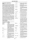
8279 is packaged in a 40 pin DIP.
The
following
is
a
functional
description
of
each pin.
No.
Of
Pins
Designation
8
2
2
4
8
DBo-DB7
ClK
RESET
CS
Ao
RD,
WR
IRQ
V
ss
,
Vee
SLo-SLa
Rlo-Rl7
Function
Bi-directional
data bus. All data
and
commands
between
the
CPU
and
the
8279 are trans-
mitted
on
these lines.
Clock
from
system used
to
gen-
erate
internal
timing.
A
high
signal
on
this
pin
resets
the
8279.
After
being
reset
the
8279
is
placed
in
the
following
mode:
1)
16 8-bit
character
display
-left
entry.
2)
Encoded
scan
keyboard-2
key
lockout.
Along
with
this
the
program
clock
prescaler
is
set
to
31.
Chip
Select. A
low
on this pin
enables
the
interface
functions
to
receive
or
transmit.
Buffer
Address. A
high
on this
line
indicates
the
signals in
or
out
are
interpreted
as a
com-
mand
or
status. A
low
indicates
that
they
are data.
Input/Output
read and write.
These signals enable
the
data
buffers
to
either
send data
to
the
external
bus
or
receive it
from
the
external bus.
Interrupt Request. In a keyboard
mode,
the
interrupt
line is
high
when
there
is data in
the
FIFO/
Sensor
RAM.
The
interrupt
line
goes
low
with
each
FIFO/
Sensor
RAM read and returns
high
if
there is still
informa-
tion
in
the
RAM. In a sensor
mode,
the
interrupt
line goes
high
whenever a
change
in a
sensor
is detected.
Ground
and power supply pins.
Scan
Lines
which
are used
to
scan
the
key
switch
or
sensor
matrix
and
the
display
digits.
These lines can be
either
en-
coded
(1
of
16)
or
decoded
(1
of
4).
Return
line
inputs
which
are
connected
to
the
scan lines
through
the
keys
or
sensor
switches.
They
have active
in-
ternal
pullups
to
keep
them
high
until
a
switch
closure
pulls
one
low.
They
also serve
as
an
8-bit
input
in
the
Strobed
Input
mode.
No.
Of
Pins
SHIFT
The
shift
input
status
is
stored
along
with
the
key
position
on
key
closure
in
the
Scanned
Designation
Function
CNTLlSTB
Keyboard
modes.
It
has an
ac-
tive
internal
pullup
to
keep
it
high
until
a
switch
closure
pulls
it
low.
For
keyboard
modes
this line is
used
as
a
control
input
and
stored
like
status on a key
clo-
sure. The
line
is also
the
strobe
line that enters
the
data
into
the
FIFO
in
the
Strobed
Input
mode.
(Rising Edge).
It
has an active
internal
pullup
to
keep
it
high
until
a
switch
closure
pulls
it
low.
4
OUT
Ao-OUT
A3
These
two
ports
are
the
outputs
4
OUT
Bo-OUT
B3
for
the 16 x 4
display
refresh
registers.
The
data
from
these
outputs
is
synchronized
to
the
scan lines
(Slo-Sl3)
for
multi-
plexed
digit
displays.
The
two
4
bit
ports
may be
blanked
inde-
pendently. These
two
ports
may
also be
considered
as
one
8
bit
port.
BD
Blank
Display.
This
output
is
used to
blank
the
display
during
digit
switching
or
by
a
display
blanking
command.
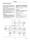
PRINCIPLES OF OPERATION
The
following
is a
description
of
the
major
elements
of
the
8279
Programmable
Keyboard/Display
interface
device.
Refer
to
the
block
diagram
in Figure 1.
1/0
Control and Data Buffers
The
I/O
control
section
uses
the
CS,
Ao,
RD
and
WR
lines
to
control
data
flow
to
and
from
the
various
internal
registers
and
buffers. All data
flow
to
and
from
the
8279 is
enabled
by
CS. The
character
of
the
information,
given
or
desired
by
the
CPU, is
identified
by
Ao.
A
logic
one
means
the
information
is a
command
Or
status. A
logic
zero means
the
information
is data. RD
and
WR
determine
the
direction
of
data
flow
through
the
Data
Buffers.
The
Data
Buffers
are
bi-directional
buffers
that
connect
the
internal
bus
to
the
external bus. When
the
chip
is
not
selected
(CS
= 1),
the
devices are in a
high
impedance
state.
The
drivers
input
during
WR
-
CS
and
output
during
RD
-CS.
Control and Timing Registers and Timing Control
These registers store
the
keyboard
and
display
modes
and
other
operating
conditions
programmed
by
the
CPU.
The
modes
are
programmed
by
presenting
the
proper
command
on
the
data lines
with
Ao
= 1
and
then
sending
a WR.
The
command
is latched
on
the
rising
edge
of
WR.
9-71
AFN-00742A-02


