M8048/M8748/M8035L
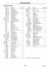
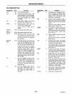
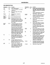
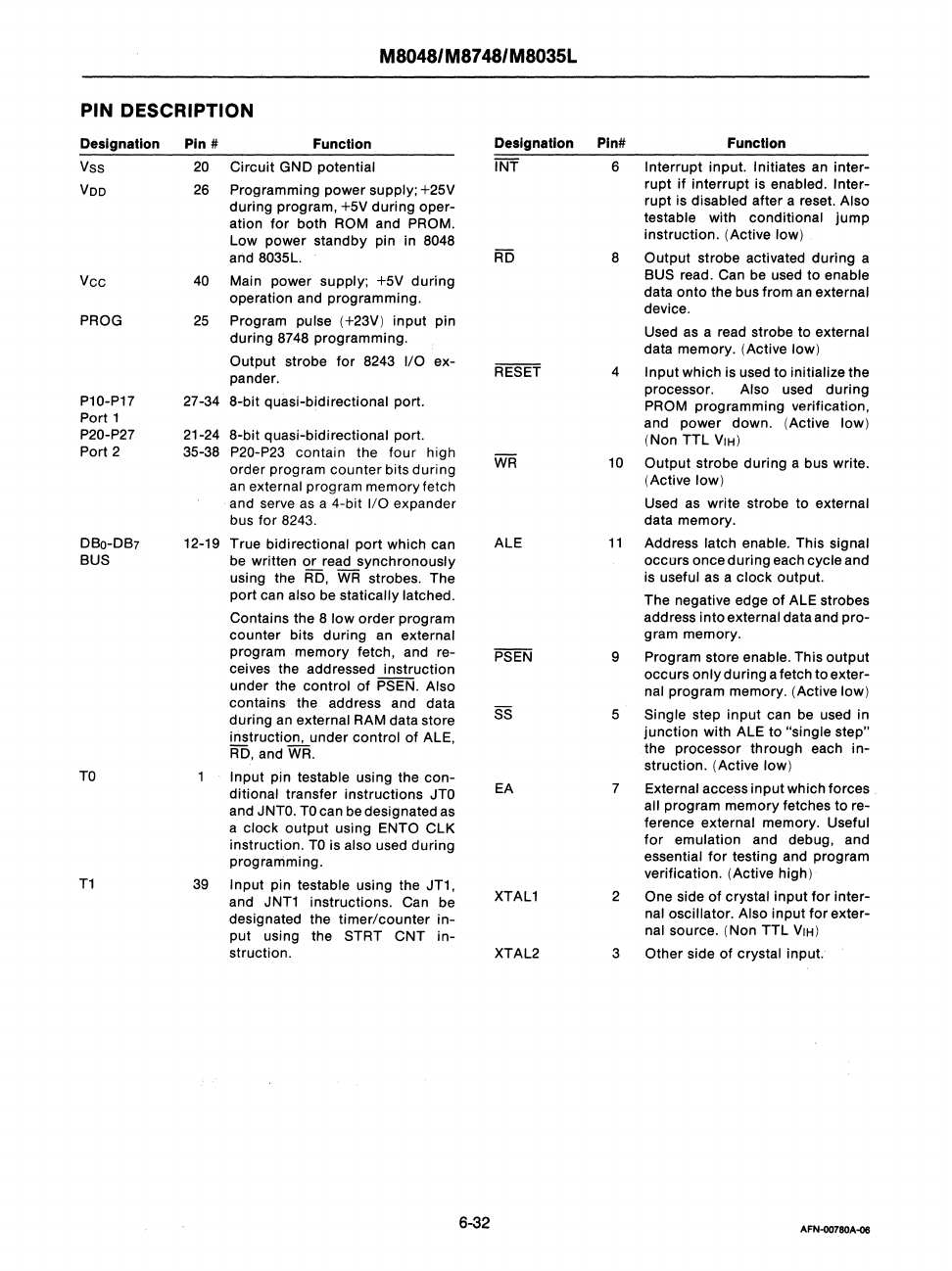
PIN DESCRIPTION
Designation
Vss
Voo
Vee
PROG
P10-P17
Port 1
P20-P27
Port 2
DBa-DB?
BUS
TO
T1
Pin
# Function
20
Circuit
GND potential
26
Programming power supply; +25V
during
program, +5V
during
oper-
ation
for
both ROM and PROM.
low
power standby pin in 8048
and 8035L.
40
Main power supply;
+5V
during
operation and programming.
25
Program pulse (+23V)
input
pin
during
8748 programming.
Output
strobe
for
8243
I/O
ex-
pander.
27-34 8-bit quasi-bidirectional port.
21-24
8-bit
quasi-bidirectional port.
35-38 P20-P23 contain the
four
high
order program
counter
bits
during
an
external program memory fetch
and serve as a 4-bit
I/O
expander
bus
for
8243.
12-19 True bidirectional
port
which can
be written
~re~synchronously
using the
RD,
WR
strobes. The
port can also be
statically latched.
Contains the 8
low
order
program
counter
bits
during
an external
program memory fetch, and re-
ceives the addressed instruction
under the
control
of
PSEN. Also
contains the address and data
during
an
external RAM data store
instruction, under
control
of
ALE
RD,
and
WR.
'
Input pin testable using the
con-
ditional transfer instructions
JTO
and
JNTO.
TO
can be designated as
a clock
output
using ENTO
ClK
instruction.
TO
is also used
during
programming.
39
Input pin testable using the JT1,
and JNT1 instructions. Can be
deSignated the
timer/counter
in-
put using the STRT
CNT
in-
struction.
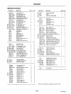
Designation
INT
ALE
EA
XTAl1
XTAl2
6-32
Pin#
Function
6 Interrupt input. Initiates
an
inter-
rupt
if
interrupt
is enabled.
Inter-
rupt is disabled after a reset. Also
testable with conditional
jump
instruction. (Active low)
8
Output
strobe activated
during
a
BUS read. Can be used to enable
data
onto
the bus from
an
external
device.
Used as a read strobe
to
external
data memory. (Active low)
4
Input
which is used
to
initialize the
processor. Also used
during
PROM programming verification,
and power down. (Active low)
(Non TTL
VIH)
10
Output
strobe
during
a bus write.
(Active low)
Used
as
write strobe
to
external
data memory.
11
Address latch enable. This signal
occurs once
during
each cycle and
is useful
as
a
clock
output.
The negative edge
of
ALE strobes
address
into
external data and
pro-
gram memory.
9 Program store enable. This
output
occurs
only
during
a fetch
to
exter-
nal program memory. (Active low)
5
Single step
input
can be used in
junction
with ALE
to
"single step"
the processor through each
in-
struction. (Active low)
7 External access
input
which forces
all program memory fetches
to
re-
ference external memory. Useful
for
emulation and debug, and
essential
for
testing and program
verification. (Active high)
2
One side
of
crystal
input
for
inter-
nal oscillator. Also
input
for
exter-
nal source. (Non
TTL
VIH)
3 Other side
of
crystal input.
AFN-00780A-<16


