


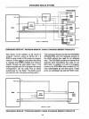

SINGLE COMPONENT SYSTEM
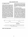
The zero cross detection capability allows the
user to make the
60
Hz
power signal the basis for
this system timing.
All
timing routines, including
time-of-day, can be implemented using the zero
cross detection capability of T 1 and its conditional
jump instructions.
In
addition, the zero cross de-
tection feature can be used
in
conjunction with the
timer interrupt
to
interrupt processing at the zero
voltage point. This enables the user to control volt-
age phase sensitive devices such as triacs and
SCRs, and to use the 8022
in
applications such as
shaft speed and
angle measurement.
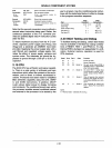
2.18 Analog
to
Digital Converter
The
8022
contains on-chip a complete hardware
implementation of
an
8-bit analog to digital
(AID)
converter with two multiplexed analog inputs.
The
A I D converter utilizes a successive approxima-
tion technique to provide
an
updated conversion
once every four instruction
cycles with a
minimum
of required software.
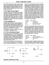
The
AID
converter consists of four
main
parts,
the input circuitry, a series string of resistors, a
voltage comparator,
and
the successive approxi-
mation logic. The two analog inputs are mUlti-
plexed
on-Chip
and
selected via software by the
SEL
ANO
and SEL
AN
1 instructions. Besides se-
lecting one of the analog inputs, these instructions
restart the conversion sequence which operates
continuously. Restarting a conversion sequence
deletes the conversion
in
progress but does not
affect the
result of the previous conversion which
is stored
in
the conversion result register. The
continuous operation of the A
I D converter saves
program space
and
time by allowing the user ob-
tain multiple readings from a given input with only
one select instruction.
To
obtain a valid conversion
reading, the user must provide the
analog input
signal
no
later than the beginning of the select
in-
struction cycle.
The
analog input is then sampled
by the A I D converter
and
maintained internally.
This voltage becomes one input to the voltage
comparator which amplifies the difference be-
tween the analog input
and
the voltage tap
on
the
series resistor string. '
The series resistor string is connected between
the
A I D
reference
pin (V
ARE
F) and ground
(AVSS). It is comprised of 256 identical resistors
which divide the
voltage between these two pins
into
256
identical voltage steps. This configuration
gives the converter its iflherent monotonicity. The
range
of
V
AREF
in
which full 8-bit resolution can be
provided is between
Vee/2
and Vee.
Thus,
the user is given a
minimum
voltage range
from ground to
V
CC
12
and
a maximum range from
ground to
Vee
over which 8-bit resolution is
in-
sured.
The
voltage tap
on
the series resistor string is se-
lected by the resistor ladder decoder. This decod-
er is driven by the 8-bit successive approximation
register (SAR). Each bit of the
SAR
is set
in
suc-
ceSSion,
MSB to LSB,
and
a voltage comparison
between the selected resistor ladder voltage and
the analog input voltage is performed after the set-
ting of each bit. The result of each comparison de-
termines whether the particular bit will remain set
or
be reset.
All
comparisons are performed auto-
matically by the
on-Chip
AID
hardware. At the end
of 8 comparisons the
SAR
contains a valid digital
result which is then latched into the conversion re-
sult
register (CRR). The
RAD
instruction (read
AID)
loads the conversion result from the
CRR
to
the accumulator of the 8022.
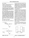
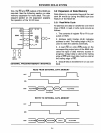
ANALOG
MULTIPLEXER
r---~
I I
I
RESISTIVE
LADDER
-
-"--~-----,
RI2
I ,
I I
R I
Ill'
I
' ''''
..
I
:
;!~
I!
I"
I
8-W
RI2
I I
L
__
L.J
8-
INTERNAL
BUS
AID CONVERTER BLOCK DIAGRAM
As mentioned previously, the software and time
required to perform
an
A I D conversion is opti-
mized by the
8022's
on-chip
AID
converter con-
figuration.
Typical
software
for
reading
two
sequential A I D conversions and storing them
in
data memory is shown below:
2-29