


inter
8031/8051/8751
1.0
INTRODUCTION
This data sheet provides
an
introduction to the
8051
family. A detailed description
of
the hardware re-
quired to expand the
8051
with more program mem-
ory, data memory,
I/O, specialized peripherals and
into
multiprocessor configurations is described in
the
8051
Family User's Manual.
1.1
THE
8051
FAMILY
The
8051
is
a stand-alone high-performance single-
chip computer intended for
use
in
sophisticated
real-time applications such
as
instrumentation,
industrial control and intelligent computer periph-
erals. It provides the hardware features, architectural
enhancements and new instructions that make
it
a
powerful and cost effective controller for applications
requiring up to 64K-bytes of program memory and/or
up to 64K-bytes
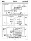
of
data storage. A Block Diagram
is
shown
in
Figure
3.
The
8031
is
a control-oriented CPU without on-chip
program memory. It can address 64K-bytes
of
external Program Memory in addition to 64K-bytes
of
External Data Memory. For systems requiring extra
capability, each member
of
the
8051
family can be
expanded using standard memories and the byte
oriented
MCS-80 and MCS-85 peripherals. The
8051
is
an
8031
with the lower 4K-bytes
of
Program
Memory
filled with on-chip mask programmable
ROM while the
8751
has
4K-bytes
of
UV-light-
erasable/electrically-program
mabie
ROM.
The three pin-compatible versions
of
this com-
ponent reduce development problems to a minimum
and provide maximum
flexibility. The
8751
is
well
suited for development, prototyping, low-volume
production and applications requiring field updates;
the
8051
for low-cost, high volume production; and
the
8031
for applications desiring the flexibility
of
external Program Memory which can be easily
!
64K
EXTERNAL
modified and updated in the field.
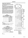
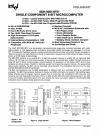
2.0 MACRO-VIEW OF THE
8051
ARCHITECTURE
On a single die the
8051
microcomputer combines
CPU; non-volatile 4K x 8 read-only program me·mory;
volatile
128 x 8 read/write data memory;
321/0
lines;
two
16-bit timer/event counters; a five-source,
two-
priority-level, nested interrupt structure; serial
I/O
port for either multi-processor communciations,
I/O
expansion,
or
full duplex UART; and on-Chip oscilla-
tor
and clock circuits. This section will provide
an
overview
of
the
8051
by
providing a high-level de-
scription
of
its major elements: the CPU architecture
and the
on-chip
functions peripheral
to
the CPU.
The generic term ".8051"
is
used to refer collectively
to the 8031,8051, and 8751.
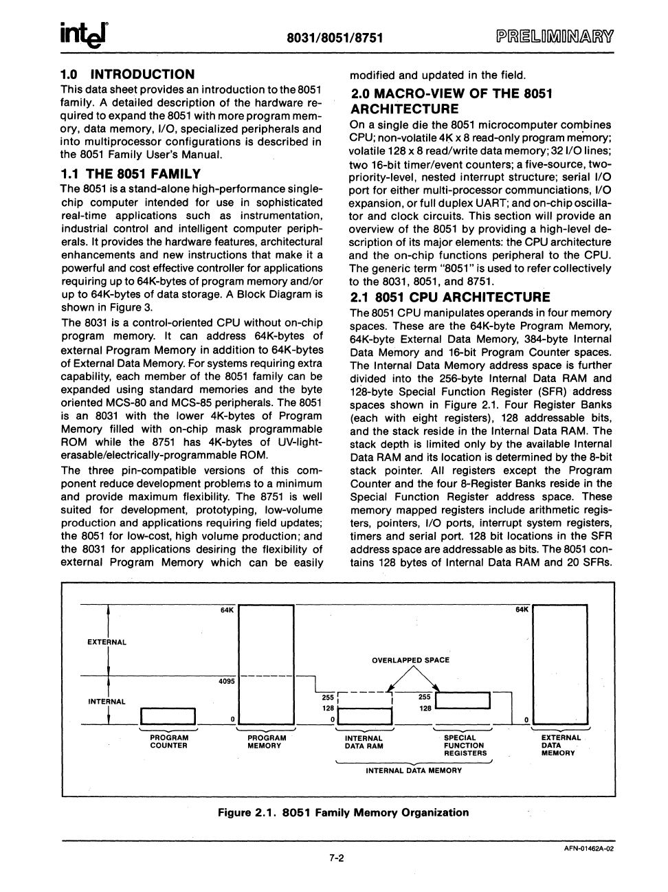
2.1
8051
CPU ARCHITECTURE
The
8051
CPU manipulates operands in four memory
spaces. These are the 64K-byte Program Memory,
64K-byte
External Data Memory, 384-byte Internal
Data Memory and 16-bit Program Counter spaces.
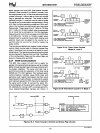
The Internal Data Memory address space
is
further
divided into the 256-byte Internal Data RAM and
128-byte Special Function Register
(SFR)
address
spaces shown in Figure
2.1.
Four Register Banks
(each with eight registers),
128
addressable bits,
and the stack reside in the
Internal Data RAM. The
stack depth
is
limited only by the available Internal
Data RAM and its location
is
determined by the 8-bit
stack pointer.
All registers except the Program
Counter and the four 8-Register Banks reside in the
Special Function Register address space. These
memory mapped registers include arithmetic regis-
ters, pointers,
I/O ports, interrupt system registers,
timers and
serial port.
128
bit locations in the
SFR
address space are addressable
as
bits. The
8051
con-
tains
128
bytes
of
Internal Data RAM and
20
SFRs.
64K
OVERLAPPED
SPACE
I
-------
~r-----A
4095
Il
INTERNAL
255
I I 255
I
12:
I I 128
I
PROGRAM
COUNTER
I
0
~
PROGRAM
MEMORY
'----...------'
INTERNAL
DATA RAM
'----...------'
SPECIAL
FUNCTION
REGISTERS
INTERNAL DATA MEMORY
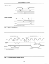
Figure 2.1.
8051
Family Memory Organization
,
EXTERNAL
DATA
MEMORY
,
AFN-01462A-Q2