


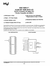

8755A
ERASURE
CHARACTERISTICS
The erasure characteristics of the 8755A are such that
erasure begins to
occur
when exposed to light with
wavelengths shorter than approximately 4000 Angstroms
(AI. It should
be
noted that sunlight and certain types of
fluorescent lamps have wavelengths in the
3000-4000A
range. Data show that constant exposure to room level
fluorescent lighting could erase the typical 8755A in
approximately 3 years while it would take
approxill1ately 1
week to cause erasure when exposed to direct sunlight.
If the 8755A is to
be
exposed to these types
of
lighting
conditions for extended periods of time, opaque labels
are available from
Intel which should be placed over the
8755 window to prevent unintentional erasure.
The recommended erasure procedure for the 8755A is
exposure to shortwave ultraviolet light which has a wave-
length
of
2537 Angstroms (AI. The integrated dose Ii.e.,
UV
intensity X exposure time) for erasure should
be
a
minimum
of
15W-sec/cm2. The erasure time with this
dosage is approximately
15
to 20 minutes using an ultra-
violet lamp with a
12000",W/cm
2
power rating. The
8755A should
be
placed within one inch from the lamp
tubes during erasure. Some lamps have a filter on their
tubes and this filter should
be
removed before erasure.
PROGRAMMING
Initially, and after each erasure, all bits
of
the EPROM
portions of the 8755A are in the "1" state. Information
is
introduced by selectively programming "0" into the
desired bit locations. A programmed
"0" can
only
be
changed to a
"1"
by UV erasure.
The 8755A can be programmed on the
Intel® Universal
PROM Programmer (UPPI, and the PROMPT'" 80/85 and
PROMPT-48'" design aids. The appropriate programming
modules and adapters
for
use in programming both
8755A's
and
8755's are shown
in
Table
1.
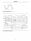
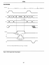
The program mode itself consists
of
programming a
single address at a time, giving a
Single
50
msec pulse
for
every address. Generally, it is desirable to have a
verify cycle after a program cycle for the same address
as
shown in the attached timing diagram.
In
the verify
cycle (i.e., normal memory read cycle I
'Voo'
should
be at
+5V.
Preliminary
timing
diagrams and parameter values per·
taining
to
the 8755A programming operation are con·
tained in Figure
6.
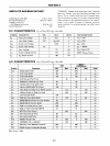
TABLE
1.
875SA PROGRAMMING MODULE CROSS
REFERENCE
MODULE NAME
UPP
955
UPP
UP2121
PROMPT 975
PROMPT 475
NOTES:
USE WITH
UPPI41
UPP
855
PROMPT
80/85131
PROMPT
48(
11
1,
Described on
p.
11·9
of 1978 System Data Catalog.
2.
Special adaptor socket.
3.
Described on
p.
11·3
of
1978
System Data Catalog.
4.
Described on
p.
10·85
of
1978 System Data Catalog.
6-76
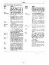
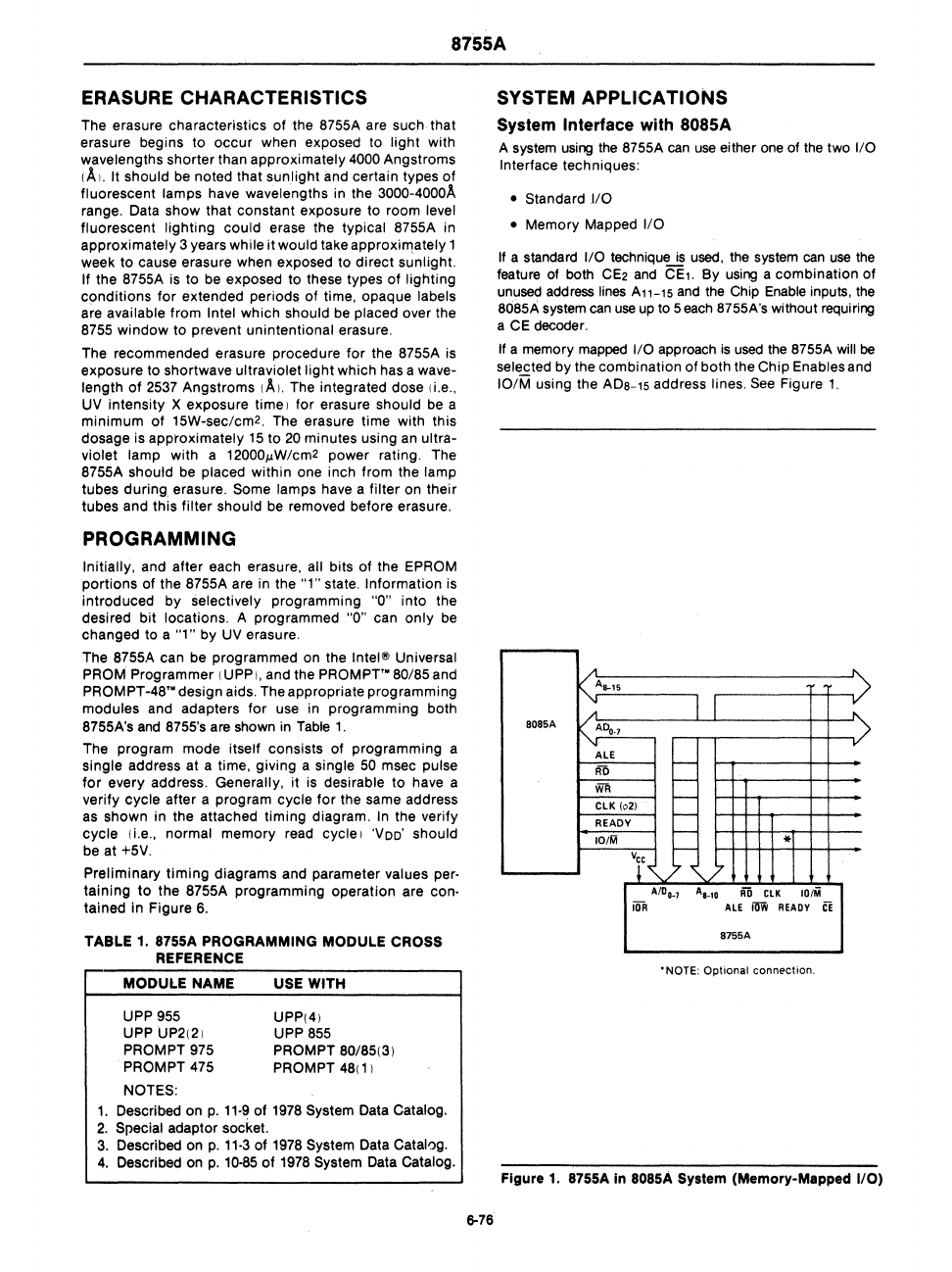
SYSTEM
APPLICATIONS
System Interface with
SOSSA
A system
using
the
8755A
can
use
either
one
of
the
two I/O
Interface
techniques:
• Standard
I/O
• Memory Mapped
I/O
If a standard
I/O
technique
is
used,
the system
can
use
the
feature
of
both
GE2
and
CE1.
By
using
a combination of
unused address
lines
A11-15
and
the
Chip
Enable
inputs,
the
8085A system
can
use
up
to 5
each
8755A's without requiring
a
CE decoder.
If a memory
mapped
I/O
approach
is
used
the
8755A will
be
selected by the combination
of
both the Chip Enables and
10/M using the AD8-15 address lines.
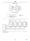
See
Figure
1.
/1
"
1~8-15
~
BOB5A
MO
o
.
7
"
V
ALE
-
RO
WR
;---
elK
102)
r--
REAOY
r--
101M
r--
*1
Vee
;---
I
rV
'\..
7
AID,.,
A'_10
RD
elK
101M
iifR
ALE
ilii'i
READY
CE
B755A
'NOTE: Optional connection.
Figure
1.
8755A
in
808SA System (Memory-Mapped
1/0)