SINGLE COMPONENT SYSTEM
the
..
counter increments
to
its maximum
count
(FF),
and overflows
to
zero. The count
continues until stopped
by
a STOP
TCNT
instruction
or
RESET.
The
increment from
maxini"um
..
count
to
zero (overflow) sets
an
overflow flag. The state
of
the overflow flag
is testable with the conditional
jump
in-
struction JTF. The flag is reset
byJTF
but
not
by executing a RESET, unlike the 8748.
Bya
MOV T,A instruction, the contents
of
the
accumulator are loaded
to
the timer.
At
the STRT T command an internal prescaler
is zeroed and thereafter increments once
each
30
input
clocks (once each single
cycle instruction, twice each double cycle
instruction>. The prescaler is a divide by
32.
At
the
(11111)
to
(00000>
transition the
timer
is incremented. The timer is 8-bits and an
overflow (FFH)
to
(OOH)
timer flag is set. A
conditional branch instruction (JTF) is
available
for
testing this flag, the flag being
reset each test. Total
count
capacity
forthe
timer
is
28
x
25
= 8192
or
81.9 msec at a
10
Msec
cycle time. Contents of
the.
timer are
moved to the accumulator by the
MOV A,T
instruction
without
disturbing the counting
process. The
timer
stops upon the STOP
TCNT
instruction.
The
STRT
CNT
instruction connects the
T1
input
pin
to
the event counter input and
enables the counter. Subsequent
high-to-
low
transitions on
T1
increment the
counter. The maximum rate at which the
counter can increment is once per three
instruction cycles
(30MS
for
a 3 MHz
oscillator>. There is no minimum frequency.
T1
input must remain high
for
at least 500ns
after each transition. The event counter is
stopped by a
STOP
TCNT
instruction.
2.9 Input/Output Capabilities
The
8021
I/O configurations are
highly
flexible. A
number
of
different
configur-
ations are possible, tailoring
an
8021
to
a
given task.
Other than the power supply
and dedicated pins, all other pins
(20)
can
be used
for
input, output,
or
both,
depending on the configuration.
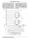
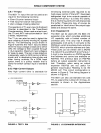
All ports are quasi-bidirectional to facili-
tate stand-alone use. A simplified sche-
matic
of
the quasi-bidirectional inter-
face is shown in Figure
3.
This
con-
figuration allows buffered
output~,
and
also allows external input. Data written
to
these ports is statically latched and remains
unchanged until rewritten. As
input
ports
these lines are non-latching, i.e., inputs
must be present until read
by
an
input
instruction. When writing a
"0"
or
low
value
to
these ports, the large
pulldown
device
sinks an external
TTL
load. When writing a
"1", a large current is supplied
through
the
large
pullup
device to allow a fast data
transfer. After a short time (less than one
instruction cycle), the large device is
shut
off
and the small pullup maintains the
"1"
level indefinitely. However, in this situation,
an
input
device capable
of
overriding the
small
amount
of
sustaining current sup-
plied by the pullup device can be
read,
(Alternatively, the data written
ca"n
be
read>'
So, by writing a
"1"
to
any particular pin,
that
pin can serve either
as
a true high:-Ievel
latched
output
pin,
or
as
just
a
pullup
resistor on
an
input. This allows maximum
user flexibility in selecting his
input
or
latched
output
pins, with a minimum
of
external components.
Port
00-07 is also quasi-bidirectional,
except there
is
no large pullup device. As
outputs, this
port
is essentially open drain.
By mask option the small pullup devices on
POO-P07
may be deleted on any pin
providing a true open drain output. This is
useful in driving analog circuits and certain
loads, such
as
keyboards.
2-22
INPUT
BUFFER
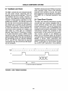
FIGURE
3.
QUASI-BIDIRECTIONAL
PORT STRUCTURE


