8255A18255A·5
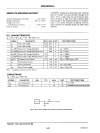
ABSOLUTE MAXIMUM RATINGS·
Ambient
Temperature Under
Bias
.........
o°c
to 70°C
Storage Temperature
..............
_65°C
to
+150°C
Voltage
on
Any
Pin
With Respect
to
Ground .
.....
-0.5V
to
+7V
Power Dissipation.
.
. . . . . . . . . . . . . . . 1 Watt
D.C.
CHARACTERISTICS
TA
=
o°c
to 70°C. Vee =
+5V
±5%; GND =
ov
SYMBOL
PARAMETER
MIN.
VIL
Input
Low Voltage
-0.5
VIH
Input High Voltage
2.0
VOL
(DB)
Output
Low Voltage (Data
Bus)
VOL (PER)
Output
Low Voltage (Peripheral Port)
VOH(DB)
Output
High Voltage (Data Bus)
2.4
VOH(PER)
Output
High Voltage (Peripheral Port)
2.4
IDAR[11
Darlington Drive Current
-1.0
lee
Power Supply Current
IlL
Input
Load Current
IOFL
Output
Float
Leakage
Note
1:
Available
on
any
8
pins
from
Port
Band
e.
CAPACITANCE
TA
=25°C;Vee=GND=OV
SYMBOL
PARAMETER
MIN.
TYP.
CIN
Input Capacitance
CliO
I/O
Capacitance
'COMMENT:
Stresses
above
those
listed under "Absolute
Maximum Ratings" may
cause
permanent
damage
to
the
device.
This
is
a
stress
rating only and functional opera·
tion
of
the device
at
these
or
any other conditions above
those
indicated in
the
operational sections
of
this specifi·
cation
is
not
implied. Exposure to absolute maximum
rating conditions
for
extended periods may
affect
device
reliability.
MAX.
UNIT
TEST CONDITIONS
0.8
V
Vee
V
0.45 V
IOL = 2.5mA
0.45 V
IOL
=1.7mA
V
IOH
= -400!-LA
V
IOH
=
-200!-LA
-4.0
mA
REXT
=
750n;
VEXT=
1.5V
120
mA
±10
!-LA
VIN
= Vee
to
OV
±10
!-LA
VOUT
= Vee
to
OV
MAX.
UNIT
TEST
CONDITIONS
10 pF fc = 1MHz
20
pF
Unmeasured pins returned
to
GN
~:O~'~
LJ
l
~_~
: y
y--------.,..
VEXT"
I 100pF
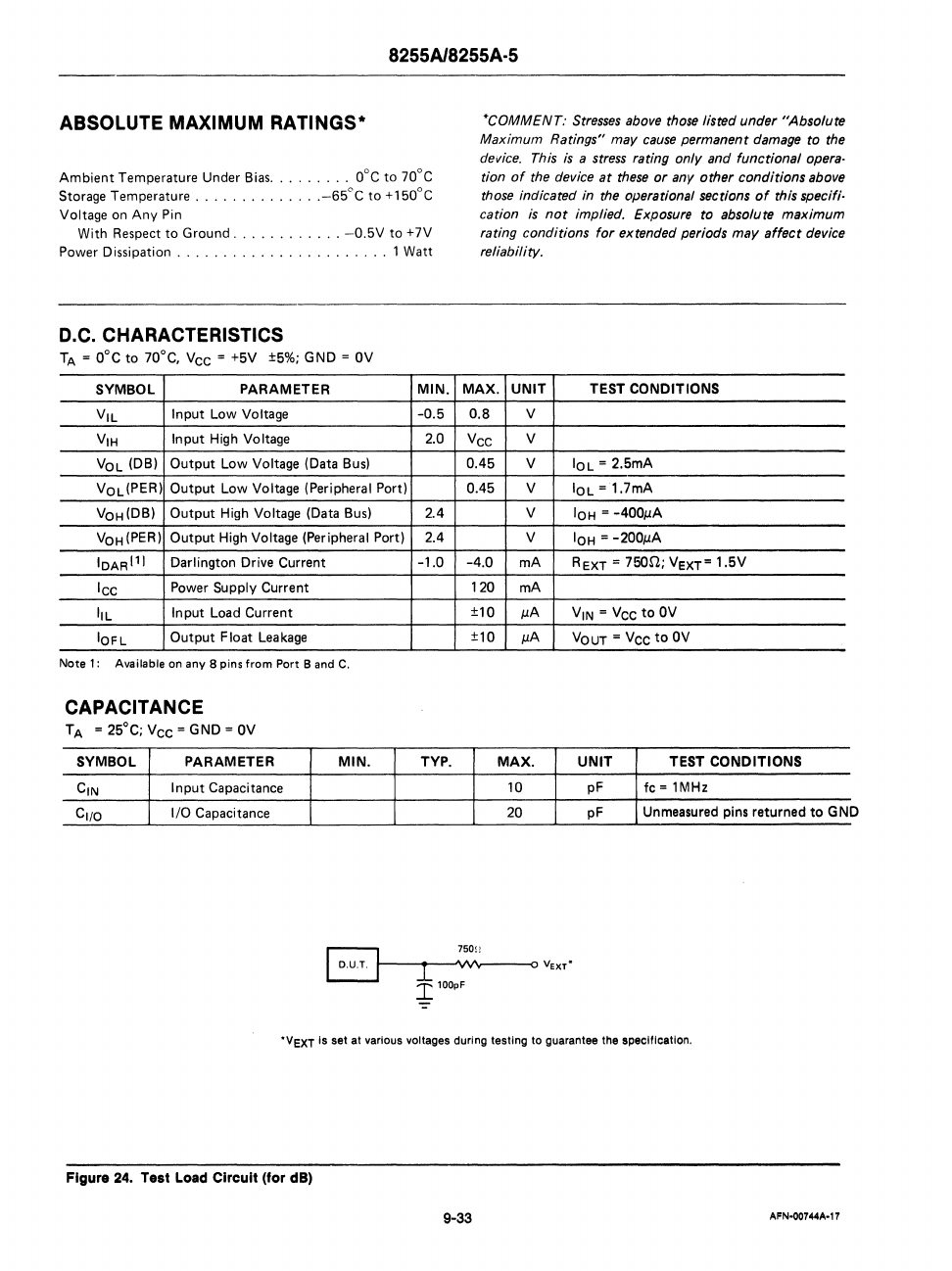
'VEXT
Is
set
at
various
voltages
during
testing
to
guarantee
the
specification.
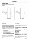
Figure
24.
Test Load
Circuit
(for dB)
9-33
AFN·00744A·'7
o


