8185/8185-2
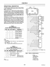
OPERATIONAL DESCRIPTION
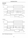
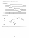
The 8185 has been designed to provide for direct interface
to the
multiplexed bus structure and bus timing of the
8085A microprocessor.
At the beginning of
an
8185 memory access cycle, the 8-
bit address on ADo-7,
As
and
Ag,
and the status of CEI and
CE2
are all latched internally in the
8185
by the falling edge
of ALE.
If the latched status of both CEI and
CE2
are
active, the 8185 powers
itself up, but no action occurs until
the
CS
line goes low and the appropriate
RD
or
WR
control
signal
input is activated.
The
CS
input is not latched by the
8185
in order to allow
the maximum amount
of
time for address decoding in
selecting the 8185 chip. Maximum power consumption
savings
will occur, however, only when CEI and
CE2
are
activated
selectively to power down the 8185 when it
is
not
in
use.
A possible connection would
be
to wirethe 8085A's
101M
line to the 8185's CEI input, thereby keeping the
8185 powered down during
1/0
and interrupt cycles.
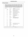
TABLE 1.
TRUTH TABLE
FOR
POWER DOWN AND FUNCTION ENABLE
CE
1
CE
2
CS
{CS*)[2]
8185 Status
1
X X
0
Power Down and
Function
Disablell]
X
0 X
0
Power Down and
Function
Disable[l]
0
1 1
0 Powered Up and
Function
Disable[l]
0
1
0
1 Powered Up and
Enabled
Notes:
X:
Don't Care.
1:
Function Disable implies Data Bus in high impedance state
and not writing.
2:
CS'
= (CEI =
0)
•
(CE2
=
1)
• (CS =
0)
CS· = 1 signifies all chip enables and chip select active
(CS*)
0
1
1
1
Note:
TABLE
2.
TRUTH TABLE
FOR
CONTROL AND DATA BUS PIN STATUS
ADo_7
During Data
RD
WR
Portion of Cycle 8185 Function
X X Hi-Impedance
No Function
0 1
Data from Memory Read
1
0
Data to Memory
Write
1 1 Hi-Impedance
Reading, but not
Driving Data Bus
X:
Don't Care.
6-97
-
-
-
-
-
-
r1D~
Vss
Vee
I
I I
TRAP
X,
X,
RESET IN
-
HOLD
RST7,5
HLDA
--
AST6,S
8085A
SOD
'--
RST5,5
SID
-
INTR
9,
r--
1NTA
RESET
9
0
-
ADDRi
OUT
ADDR
DATA ALE Ali
WIi
101M
ROY
eLK
,81
,81
VI'
T
H-
~
POR~~
WR
~
_ PORT (8)
R0
8156
B
ALE
'ORTP(>
DATAl
c (6)
ADDR
"
IN
101M
TIMER
~
RESET OUT
lOW
Ali
ALE
p(>
PORT
Il-r-
CE
A
~~
"-
A
s
.
10
V
8355/
8755A
DATAl
ADDR
101M
p(>
PORT
RESET
8
ROV
~
eLK
vs!
v!c
V~D
tROG
WR
RO
CE,
8185
ALE
H--
es,
CE
2
H--
As,
Ag
ADQ.7
vL
vL
Vee
Vee
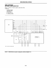
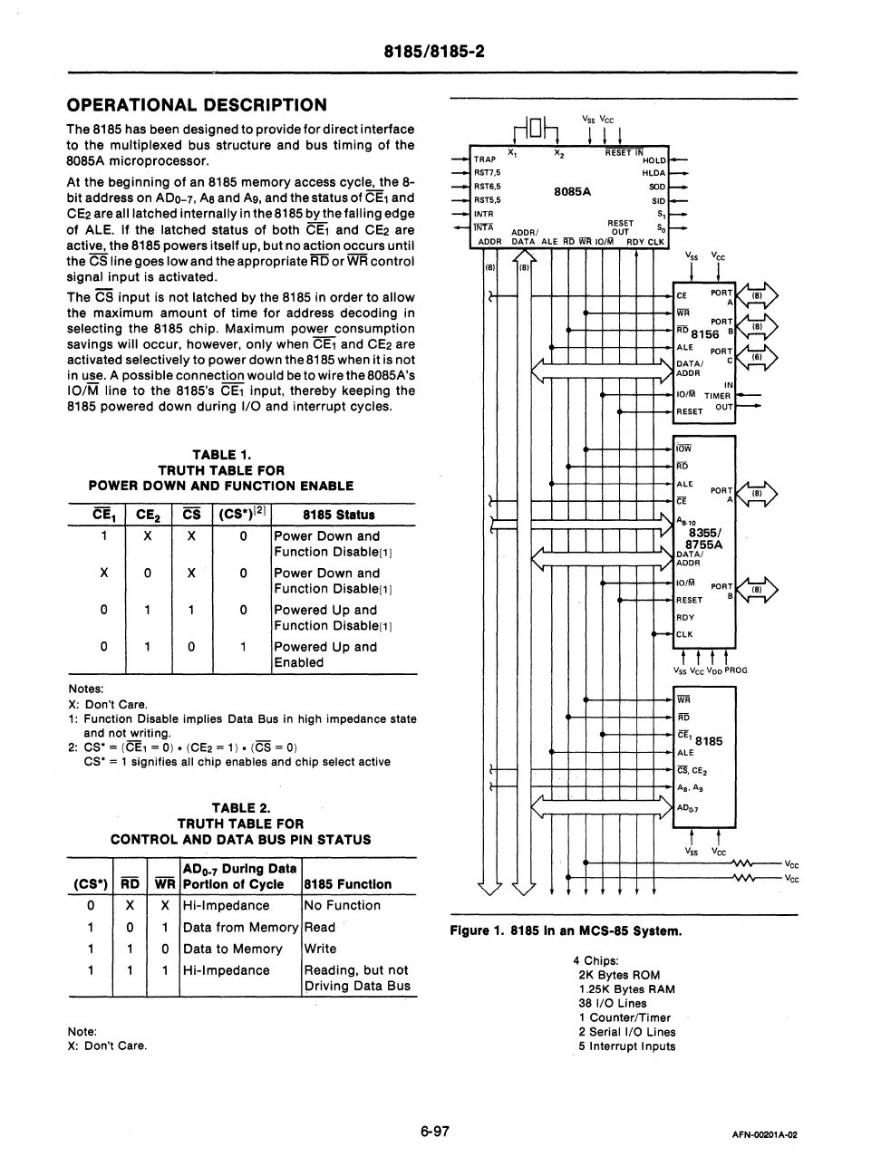
Figure 1. 8185
in
an
MCS-85 System.
4 Chips:
2K
Bytes ROM
1 .25K Bytes RAM
38
I/O
Lines
1 Counter/Timer
2 Serial I/O Lines
5
Interrupt Inputs
AFN-00201 A-02


