8041
AJ8641AJ8741
A
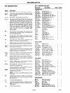
PIN DESCRIPTION
Signal Description
0
0
-
0
7
Three·state, bidirectional DATA
BUS BUFFER lines
(BUS)
used
to
interface the UPI·41A
to
an 8·bit master
system data bus.
P
10
-P
17
8·bit, PORT 1
quasi·bidirectionall/O
lines.
P
20
-P
27
8·bit, PORT 2
quasi·bidirectionall/O
lines. The lower
4
bits
(P
20
-P
23
) interface
directly
to
the 8243 I/O ex·
pander device and contain address and data infor·
mation
during
PORT
4-7
access. The upper 4
bits
(P
24
-P
27
) can be programmed
to
provide Interrupt
Request and DMA Handshake capability. Software
control
can
configure
P
24
as
OBF
(Output Buffer
Full), P
25
as IBF (Input
Buffer
Full~as
DRQ
(DMA
Request),
and
P
27
as
DACK
(DMA
ACKnowledge).
WR
I/O write
input
which enables the master CPU
to
write data and command words
to
the UPI·41A IN·
PUT DATA BUS BUFFER.
RD
110
read input which enables the master
CPU
to
read data and status words from the
OUTPUT DATA
BUS BUFFER
or
status register.
CS
Chip select input used
to
select one UPI·41A
out
of
several connected to a common data bus.
Ao
Address input used by the master processor
to
in·
dicate whether byte
transfer
is data
or
command.
TEST
0,
Input pins which can be
directly
tested using condi·
TEST 1 tional branch
instructions.
T1
also
functions
as the event
timer
input (under
software control).
To
is used
during
PROM program·
ming and verification in the 8741A.
XTAL
1,
Inputs
for
a crystal,
LC
or
an
external timing signal
XTAL2
to
determine the internal
oscillator
frequency.
SYNC
Output
signal which
occurs
once per UPI·41A in·
struction
cycle. SYNC can be used as a strobe
for
external circuitry; it is also used
to
synchronize
single step operation.
EA
External access input which allows emulation,
testing and
PROM/ROM verification.
PROG
Multifunction
pin used as the program pulse input
during
PROM
programming.
During
I/O expander access the PROG pin
acts
as
an
address/data strobe
to
the 8243.
RESET Input used to reset
status
flip·flops
and to set the
program
counter
to
zero.
RESET is also used
during
PROM programming and
verification.
SS Single step input used in the 8741A in
conjunction
with
the SYNC
output
to
step the program through
each
instruction.
Vee
Voo
Vss
+
5V
main power supply pin.
+ 5V
during
normal operation. + 25V during pro·
gramming operation. Low power standby pin in
ROM
version.
Circuit
ground potential.
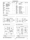
UPITM
INSTRUCTION
SET
Mnemonic
Description
Bytes Cycles
ACCUMULATOR
ADD
A.Rr
ADD
A.@Rr
ADD
A.#data
ADDC
A.Rr
ADDC
A.@Rr
ADDC
Mdata
ANL
A.Rr
ANL
A.@Rr
ANL
A.#data
ORl
A.Rr
ORL
A.@Rr
ORL
A.#data
XRl
A.Rr
XRL
A.@Rr
XRL
A.#data
INC
A
DEC
A
CLR
A
CPL
A
DA
A
SWAP
A
RL
A
RlC A
RR
A
RRC
A
INPUT
/OUTPUT
IN
A.Pp
OUTL
Pp.A
ANl
Pp.#data
ORl Pp.#data
IN
A.DBB
OUT
DBB.A
MOV
STS,A
MOVD
A.Pp
MOVD
Pp.A
ANlD
Pp.A
ORlD
Pp.A
DATA
MOVES
Add
register
to
A
Add
data memory
to
A
Add
immediate
to
A
Add
register
to
A with carry
Add
data
memory
to
A with carry
Add
immed.
to
A with carry
AND
register
to
A
AND
data memory
to
A
AND
immediate
to
A
OR
register
to
A
OR
data memory
to
A
OR
immediate
to
A
Exclusive
OR
register
to
A
Exclusive
OR
data memory
to
A
Exclusive
OR
immediate
to
A
Increment A
Decrement
A
Clear A
Complement A
Decimal
Adjust A
Swap
nibbles
of
A
Rotate
A left
Rotate
A left through carry
Rotate
A right
Rotate
A right through carry
Input port
to
A
Output A
to
port
AND
Immediate
to
port
OR
immediate
to
port
Input
DBB
to
A.
clear
IBF
Output A
to
DBB.
set
OBF
A4-A7
to
Bits
4-7
of
Status
Input Expander port
to
A
Output A
to
Expander port
AND
A
to
Expander port
OR
A
to
Expander port
MOV
A.Rr
Move
register
to
A
MOV
A.@Rr
Move
data memory
to
A
MOV
A.#data
Move
Immediate
to
A
MOV
Rr.A
Move
A
to
register
MOV
@Rr.A
Move
A
to
data memory
MOV
Rr.#data
Move
immediate
to
register
MOV
@Rr.#data
Move
Immediate
to
data memory
MOV
A.PSW
Move
PSW
to
A
MOV
PSW.A
Move A
to
PSW
XCH
A.Rr
Exchange A
and
register
XCH
A.@Rr
Exchange A
and
data memory
XCHD
A.@Rr
Exchange digit
of
A
and
register
MOVP
A.@A
Move
to A from current
page
MOVP3.
A.@A
Move
to
A from
page
3
TIMER/COUNTER
MOV
A.T
MOV
T.A
STRT
T
STRT
CNT
STOP
TCNT
EN
TCNTI
DIS
TCNTI
9-125
Read
Timer/Counter
Load
Timer /Counter
Start Timer
Start Counter
Stop Timer /Counter
Enable
Timer /Counter Interrupt
Disable Timer /Counter Interrupt
1
1
2
1
1
2
1
1
2
1
1
2
1
1
2
1
1
1
1
1
1
1
1
1
1
1
1
2
1
1
2
2
1
1
1
1
1
1
1
1
1
2
1
1
2
1
1
2
1
1
2
1
1
2
1
1
1
1
1
1
1
1
2
2
2
2
1
1
1
2
2
2
2
1
1
2
1
1
2
2
1
1
1
1
1
2
2
00188A


