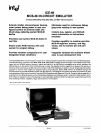
EM2
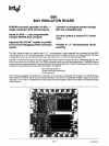
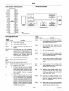
40·PIN
SOCKET
CONFIGURATION
P28
P27
AVec
VAREF
ANI
ANO
AVss
TO
VTH
POO
POI
P02
P03
P04
P05
P08
P07
ALE
Tl
Vss
Vee
P25
P24
PROD
P23
P22
P21
P20
P17
P18
P15
P14
P13
P12
Pll
Pl0
RESET
XTAL2
XTALI
SUBST
o
4(J.PIN
SOCKET
o
PIN
1
SQUARE
SOLDER
PAD
PIN DESCRIPTION
Deslg·
nation Pin II Function
Vss
20
Circuit
GND
potential.
Vcc
PROG
POO-P07
Port 0
40
+
5V
circuit power supply.
37
Output strobe for
Intell!>
8243
I/O
ex-
pander.
10-17 8·bit open-drain port with comparator
Inputs.
The
switching threshold is set
externally by V
TH
. Optional pull-up
reo
slstors
may
be
added via
ROM
mask
selection.
(The
emulator board
has
switch selection of this option.)
V
TH
9 Port 0 threshold reference pin.
P10-P17 25-32 8-bit quasi·bidirectlonal port.
Port 1
P20-P27 33-36 8-bit quasi-bidirectional port.
Port 2 38-39
P20-P23 also serve
as
a 4-bit
I/O
ex-
1-2 pander for
Intell!>
8243.
TO
8 Interrupt input
and
input pin testable
using the conditional transfer
Instruc-
tions
JTO
and
JNTO.
Initiates
an
inter-
rupt following a low level input
if
inter-
rupt is enabled. Interrupt
Is
disabled
after a reset.
T1
19
Input pin testable using the
JT1
and
JNT1
conditional transfer instructions.
Can
be
designated the timer/event
counter input using the
STRT
CNT
in-
struction. Also serves
as
the zero-cross
detection input to
allow zero-crossover
sensing of
slowly moving
AC
Inputs.
Optional pull-up resistor
may
be
added
via
ROM
mask selection.
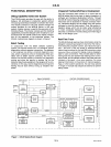
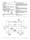
EM2
BLOCK
DIAGRAM
8022
EMULATOR
CHIP
Deslg·
2048
EPROM
.----r-l
MEMORY
8755A
nation Pin II
Function
RESET
AVss
AVcc
SUBST
V
AREF
ANO,
AN1
ALE
XTAL1
XTAL2
10-21
24
Input used to Initialize the processor
by clearing status
flip-flops
and
setting
the program counter to
zero.
7
3
21
A/D
converter GND potential. Also
establishes the lower limit of the con-
version
range.
AID
+
5V
power supply.
Substrate pin used with a bypass
capa-
citor to stabilize the substrate voltage
and
improve
AID
accuracy.
4
AID
converter reference voltage. Estab-
lishes the upper limit of the conversion
range.
6,5
Analog inputs to
AID
converter. Soft-
ware
selectable on-chip via
SEL
ANO
and
SEL
AN1
instructions.
18
Address Latch Enable. Signal occur-
ring once
every
30
input input clocks
(once every single cycle instruction),
used
as
an
output clock.
22
One
side of crystal, inductor, or
re-
sistor input for internal oscillator. Also
Input for external frequency source.
(Not
TTL
compatible.)
23
Other side of timing control element.
This pin
Is not connected when
an
ex-
ternal frequency source is used.
AFN-OOBOOA-02


