SINGLE COMPONENT SYSTEM
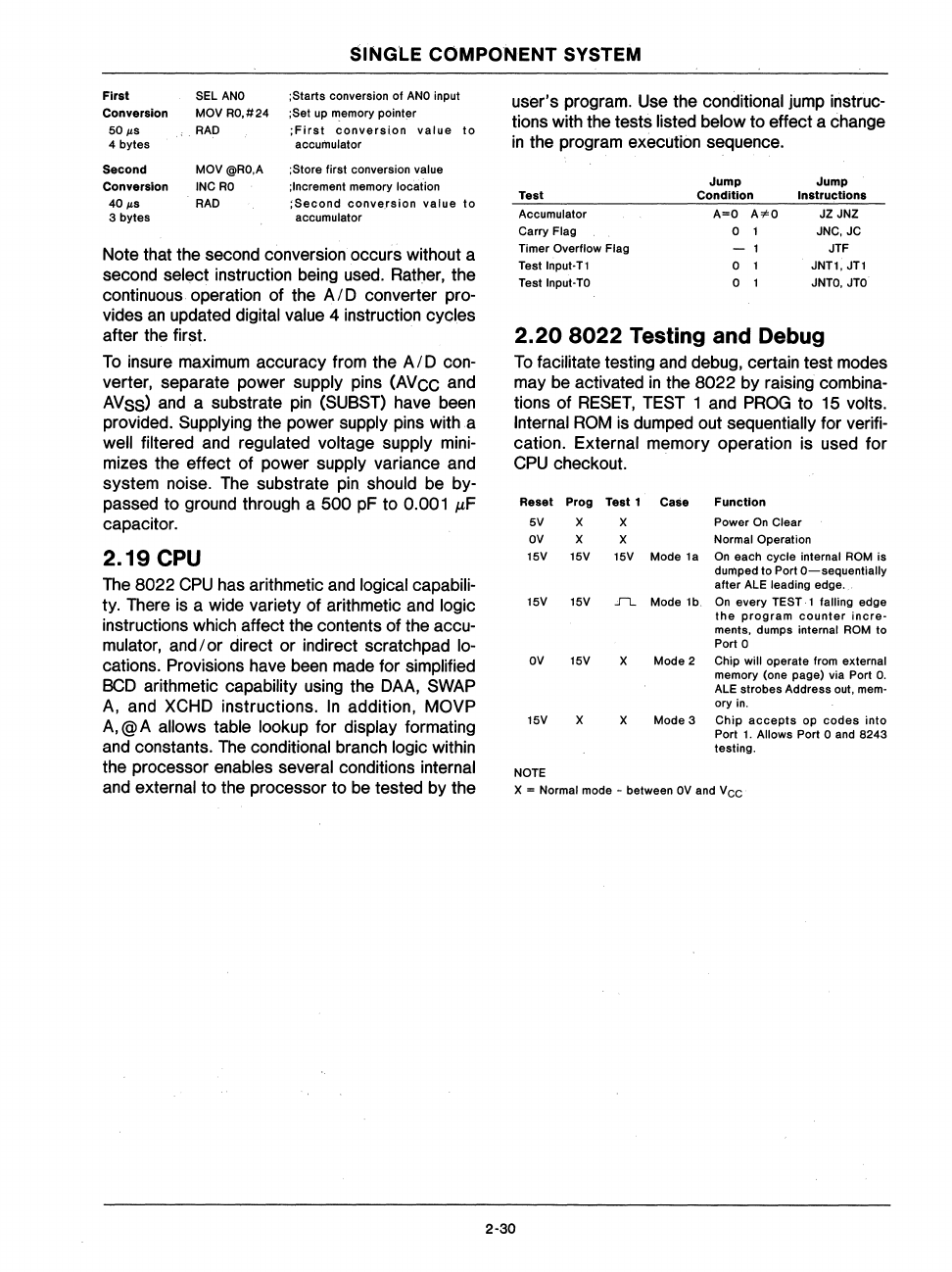
First
SEL
ANO
;Starts conversion
of
ANO
input
Conversion
MOVRO.#24
;Set
up
~emory
pointer
50/Ls
RAD
;First
conversi.on
value
to
4 bytes accumulator
Second
MOV@RO.A ;Store first conversion value
Conversion INCRO
;Increment
memory
location
40/Ls
RAD
:Second
conv8.rsion
value
to
3 bytes accumulator
Note that the second conversion occurs without a
second
select instruction being used. Rather, the
continuous operation of the A
I D converter pro-
vides
an
updated digital value 4 instruction cycles
after the first.
To
insure maximum accuracy from the
AID
con-
verter, separate power supply pins
(AVCC
and
AVSS)
and a substrate
pin
(SUBST) have been
provided.
Supplying the power supply pins with a
well filtered and regulated voltage supply mini-
mizes the effect of power supply variance and
system noise. The substrate pin
should be by-
passed to ground through a 500 pF to 0.001
f,LF
capacitor.
2.19
CPU
The 8022
CPU
has arithmetic
and
logical capabili-
ty. There is a wide variety of arithmetic and
logic
instructions which affect the contents of the accu-
mulator,
and
lor
direct or indirect scratchpad lo-
cations. Provisions have been made for simplified
BCD
arithmetic capability
using
the DAA, SWAP
A,
and XCHD instructions.
In
addition, MOVP
A,
@A allows table lookup for display formating
and constants.
The
conditional branch logic within
the processor enables several conditions internal
and external to the processor to be tested by the
user's program. Use the
conditional jump instruc-
tions with the tests listed below to effect a change
in
the program execution sequence.
Jump
Jump
Test
Condition
Instructions
Accumulator A=O
k'l'O
JZ JNZ
Carry
Flag
0
1
JNC. JC
Timer Overflow Flag
-1
JTF
Test
Input·Tl
0
1 JNT1.
JTl
Test Input·
TO
0 1
JNTO.
JTO
2.20
8022
Testing and Debug
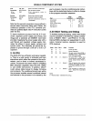
To
facilitate testing and debug, certain test modes
may be activated
in
the 8022 by
raiSing
combina-
tions of
RESET,
TEST 1 and
PROG
to 15 volts.
Internal
ROM
is dumped out sequentially for verifi-
cation.
External memory operation is used for
CPU
checkout.
Reset Prog
Te.t
1
Calie
Function
5V
X X
Power
On
Clear
OV
X X Normal Operation
15V 15V
15V Mode
la
On
each cycle internal
ROM
is
dumped to Port
O-sequentially
after
ALE
leading edge .. '
15V
15V
JL..
Mode
lb.
On
every TEST· 1 failing edge
the
program
counter
incre·
ments. dumps internal
ROM
to
Port
0
OV
15V
X
Mode 2
Chip will operate from external
memory (one page) via Port
O.
ALE
strobes Address out.
memo
ory
in.
15V
X
X Mode 3
Chip
accepts
op
codes
into
Port
1.
Allows Port 0
and
8243
testing.
NOTE
X = Normal mode - between
OV
and
Vee
2-30


