8291
INTERNAL COUNTER
The Internal counter determines the delay
time
allowed
for
the settling
of
data on the DIO lines. This delay time
is defined as
T1
In
IEEE
488
and appears in the Source
Handshake state diagram between
SDYS and
STRS.
As
such,
DAV
is asserted
T1
after the DIO lines are driven.
Consequently,
T1
is a major factor In determining the
data
transfer
rate
of
the
8291
over
the
GPIB
(T1
= TWRDV2-TWRD15).
When open-collector transceivers are used for connection
to
the GPIB,
T1
is
defined by IEEE
488
to
be
2!,sec.
8y
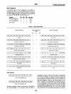
writing 0010FFFF into the Auxiliary Mode Register, the
counter
is
preset to match a
fc
MHz clock input, where
FFFF
is
the binary representation of
NF
11
SNFS8,
NF=I
FFFFI2J.·
When
NF
= fc, a 2!,sec
T1
delay will be
generated before each DAV asserted.
2NF
--
+ t
SYNC
'
1"NF,,8
fc
tSYNC
is a synchronization error, greater than zero and
smaller than the larger of T clock high and T clock
low.
I
For a
50%
duty cycle clock,
tSYNC
is less than half the
clock cyclel.
If
it
is
necessary that
T1
be
different from 2!,sec,
NF
may
be set to a value other than
fc.ln
this manner, data transfer
rates may
be
prpgrammed for a given system. In small
systems, for example, where transfer rates exceeding
GPIB specifications are required, one may set
NF
<
fc
and
decrease
T1.
When tri·state transceivers are used, IEEE
488
allows a
higher transfer rate
dower
T11.
Use
of
the
8291
with such
transceivers is enabled by setting
B2
in Auxiliary Register
B.ln this case, setting
NF
= fc causes a T 1 delay of 2!,sec to
be generated for the first byte transmitted -
all
subsequent bytes will have a delay of 500 nsec.
T11
High Speed I !,sec =
~~
+
tSYNC
Thus, setting
N'F
= 1 using
a8
MHz clock will generate
for
a
50%
duty
cycle clock
(tSYNc<63
nsec):
T1(HS)
=
2~8
+ 0.063 =
125
nsec max.
AUXILIARY
REGISTER A
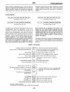
Auxiliary Register A
is
a "hidden" 5-bit register which is
used
to
enable some of the
8291
features. Whenever a
100
A4A3A2A
1
Ao
byte is written into the Auxil iary Register,
it
Is loaded with the data
A4A3A2A1Ao.
Setting the
respective bits to
"1" enables the following features:
Ao
- RFD/DAV Holdoff
on
all Data: Ifthe8291 is listening,
RFD will not
be
sent true until the "finish handshake"
auxiliary command
is
issued by the microprocessor. If the
8291
is talking, DAV is not sent true until the "finish
handshake" command is given. In both cases, the holdoff
will be in effect
for
each data byte.
A1
- RFD/DAV
Holdoff
on End: This feature enables the
holdott
on EOI
or
EOS
(if enabled). However, no holdoft
will
be
in effect on any other data bytes.
9-94
A2
- End on EOS Received: Whenever the byte in the Data
In Register matches the byte in the
EOS
Register, the End
interrupt bit
will be set
inthe
Interrupt Status 1 Register.
A3
- Output EOI on EOS
~ent:
Any occurrence of data in
the Data
Out Register matching the EOS Register causes
the
EOI line
to
be sent true along with the data.
A4
-
EOS
8inary
Compare: Setting this bit causes the
EOS
Register to function
as
a
full8·bit
word. When it is not
set, the
EOS Register is a 7·bit word
Ifor
ASCII
characters I.
If
Ao
= A, =
1,
a special "continuous Acceptor Handshake
cycling" mode is enabled. This mode should
be
used only
in a controller system configuration, where both the
8291
and the 8292 are used. It provides a continuous cycling
through the Acceptor Handshake state diagram, requiring
no
local messages from the microprocessor; the rdy local
message is automatically generated when in ANRS.
As
such, the
8291
Acceptor Handshake serves
as
the
controller Acceptor Handshake. Thus, the controller
cycles through the Acceptor Handshake, without delaying
the data transfer in progress. When the tcs
local message
is
executed, the
8291
is taken out of the "continuous
AH
cycling" mode, the
GPI8
hangs up
in
ANRS, and a
81
interrupt is generated to indicate that control may
be
taken. A simpler procedure may
be
used when a "tcs on
end of
block"
is
executed; the
8291
may stay in
"continuous
AH
cycling". Upon the end of a block (EOI
or
EOS received" a holdott
is
generated, the GPI8 hangs up
in
ANRS, and control
maybe
taken.
AUXILIARY
REGISTER B
Auxiliary Register 8 is a
"hidden" 4·bit register which is
used to enable some of the features of the
8291.
Whenever
a
101083B28180 is written into the Auxiliary Mode
Register, it
is
loaded with the data 83828,60. Setting the
respective bits to
"1" enables the following features:
Bo
- Enable Undefined Command
Pass
Through: This
feature allows any commands not recognized by the
8291
to be handled in software. If enabled, this feature will
cause the
8291
to holdott the handshake when
an
undefined command is received. The microprocessor
must then read the command from the
Command Pass
Through Register and send the
VSCMD auxiliary
command. Until the
VSCMD command is sent, the
handshake holdoff will be
in
effect.
B1
- Send EOI in SPAS: This bit enables EOI to
be
sent
with the status byte; EOI is sent true in Serial Poll Active
State. Otherwise,
EOI is sent false in
SPAS.
82
- Enable High Speed Data Transfer: This feature may
be
enabled when tri-state external transceivers are used.
The data transfer rate
is
limited by
T1
(delay time
generated in the Source Handshake function', which is
defined according to the type of transceivers used. When
the "High Speed" feature
is
enabled, T 1 = 2 microseconds
is
generated
for
the first byte transmitter! after each true
to
false transition
of
ATN. For all subsequent bytes,
T1
= 500
nanoseconds. Refer
to
the I nternal Counter section
for
an
explanation
of
T 1 duration
as
a function of
B2
and of clock
frequency.


