


inter
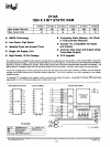
2114A FAMILY
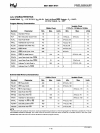
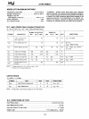
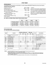
A.C. CHARACTERISTICS
TA
=
O'C
to
70'C.
Vee"
5V
±
10%.
unless otherwise noted.
READ CYCLE
(1)
2114AL-1
2114AL-2 2114AL-3
2114A-4/L-4
2114A-5
SYMBOL
PARAMETER Min. Max. Min.
Max. Min.
Max. Min.
Max. Min.
Max.
UNIT
tRC
Read Cycle Time 100
120
150
200
250
ns
tA
Access Time 100
120 150
200
250
ns
tco
Chip Selection
to
Output
Valid
70
70
70
70
85
ns
tcx
Chip Selection to Output Active 10
10
10 10
10
ns
toro
Output 3-state from Deselection
30
35
40
50
60
ns
tOHA
Output Hold from
Address Change
15
15
15
15
15
ns
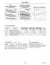
WRITE
CYCLE
[2)
2114AL-1 2114AL-2 2114AL-3.
2114A-4/L-4
2114A-S
SYMBOL
PARAMETER Min.
Max. Min. Max. Min. Max. Min. Max. Min. Max.
UNIT
twc
Write Cycle Time 100
120
150 200
250
ns
tw
Write Time
75 75
90
120
135
ns
tWR
Write Release Time
0
0 0 0 0
ns
torw
Output 3-state from Write
30
35
40
50
60
ns
tow
Data to Write Time Overlap
70 70
90
120
135
ns
tOH
Data Hold from Write Time 0
0 0
0
0
ns
NOTES:
1.
A Read occurs during the overlap of a low
Cs
and a high
WE.
2.
A Write occurs during the overlap
of
a low
CS
and a low
WE.t
w
is
measured from the latter
of
~
or
WE
going low
to
the earlier
of
CS
or
WE
going high.
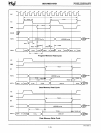
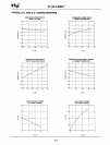
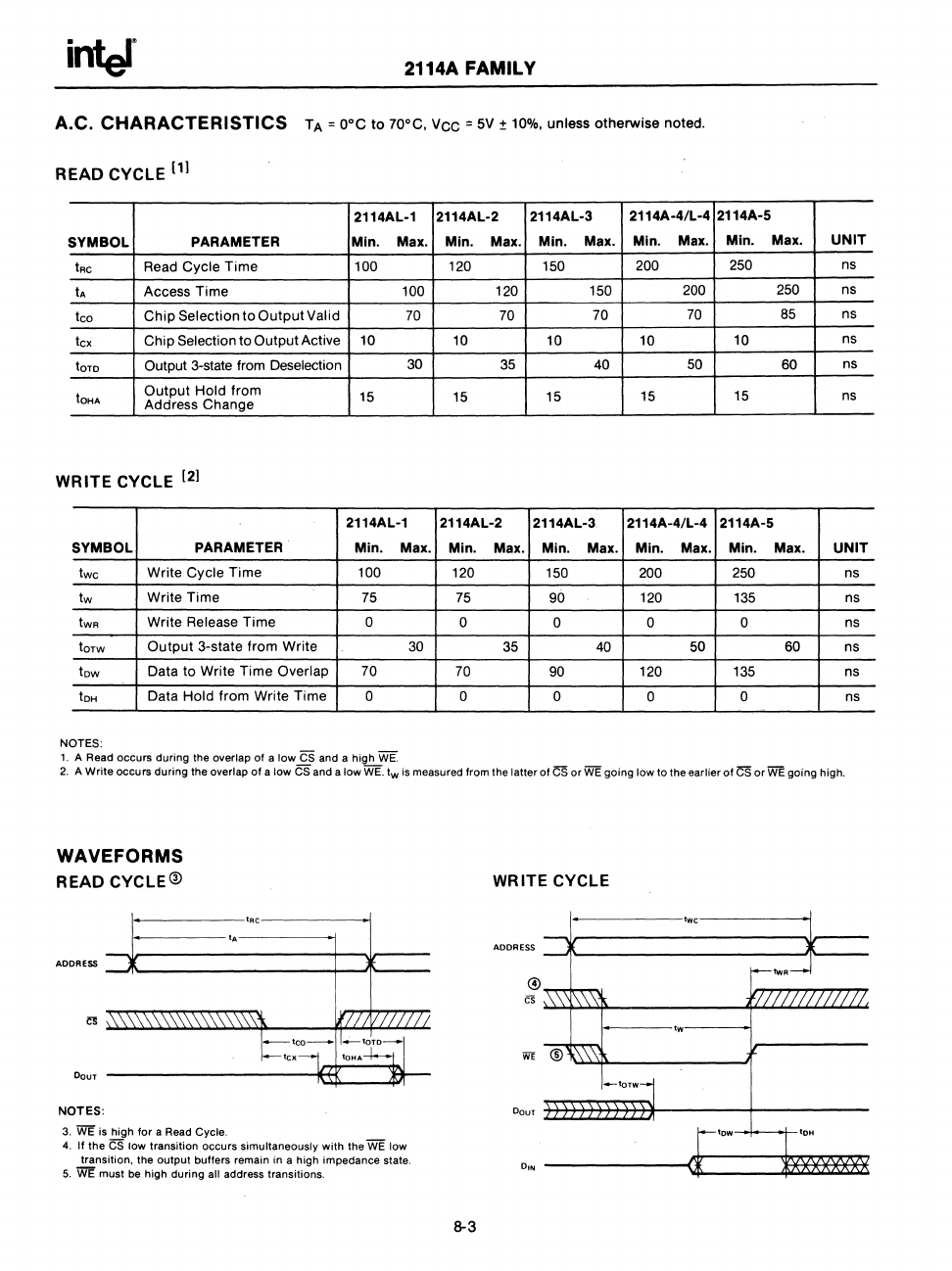
WAVEFORMS
READ CYCLE@
I------toc-------I
i------tA--------i
ADDRESS
-..II'-------------i--'l'---
NOTES:
3.
WE
is high for a Read Cycle.
4.
If
the
CS
low transition occurs simultaneously with the
WE
low
transition, the output buffers remain in a high impedance state.
5.
WE
must
be
high during all address transitions.
8-3
WRITE
CYCLE
twe
ADDRESS
~tw"-
0c~
l""""
f/I
I I
III
I
III
II,
tw
®
~\\'\
-tor=!
DOUT
[tow
_I
tDH
D,N