


8255A18255A·5
8255A FUNCTIONAL DESCRIPTION
Oeneral
The 8255A
is
a programmable peripheral interface (PPI)
device designed
for
use in
Intel~
,microcomputer
systems.
Its
function
is
that
of
a general purpose
1/0
component
to
interface peripheral equipment
to
the
microcomputer
system bus. The
functional
configura·
tion
of
the
,8255A
is programmed by the system ,software
so
that normally no external
logic
Is necessary
to
inter·
face peripheral devices or structures. '
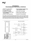
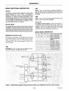
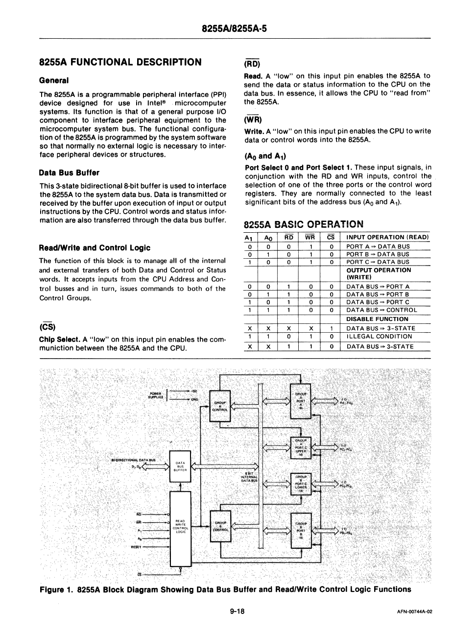
Data Bus Buffer
This 3·state
bidlrectional8·bit
buffer
is
used
to
interface
the 8255A
to
the system data bus. Data
is
transmitted
or
received by
the
buffer
upon execution
of
input
or
output
instructions
by the CPU. Control words and
status
infor·
mation
are
also
transferred through the data bus buffer.
ReadlWrl~e
and Control Logic
The function
of
this block
is
to
manage
all
of
the internal
and
external transfers
of
both
Data
and
Control or Status
words.
It
accepts
inputs from the
CPU
Address
and
Con·
trol
busses
and
in
turn,
issues
commands
to
both
of
the
Control Groups.
(CS)
Chip Select. A
"low"
on
this
input
pin enables the com·
muniction
between the 8255A and the CPU.
(RD)
Read. A
"low"
on
this
input
pin enables the 8255A
to
send the data
or
status
information
to
the CPU on the
data bus.
In essence,
it
allows
the
CPU
to
"read
from"
the 8255A.
(WR)
Write. A
"low"
on
this
input
pin enables the
CPU
to
write
data or
control
words
into
the 8255A.
(Ao
and
AI)
Port Select 0 and Port Select 1. These
input
signals, in
conjunction
with
the
RD
and WR inputs, control the
selection
of
one
of
the three ports
or
the
control
word
registers. They are normally connected
to
the least
significant
bits
of
the address bus
(Ao
and A,).
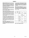
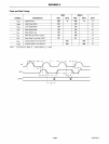
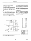
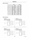
8255A
BASIC
OPERATION
Al
AO
RD
WR
CS
INPUT OPERATION
(READ)
0 0 0
,
0
PORT A ...
DATA
BUS
0 1
0 1 0 PORT
B'"
DATA
BUS
1 0 0
1 0
PORTC-DATABUS
OUTPUT
OPERATION
(WRITE)
0 0
1
0 0
DATA
BUS'"
PORT A
0 1
1
0 0
DATA
BUS'"
PORT B
1 0 1 0 0
DATA
BUS'"
PORT C
1 1 1 0 0
DATA
BUS'"
CONTROL
DISABLE
FUNCTION
X X X X
1
DATA
BUS'"
3-STATE
1 1 0 1 0
ILLEGAL
CONDITION
X X
1
1
0
DATA
BUS'"
3-STATE
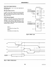
Figure 1. 82SSA Block Diagram Showing Data Bus Buffer and Read/Write Control Logic Functions
9-18
AFN-00744A-()2