SINGLE
COMPONENT
SYSTEM
PORT
0
I/O
STRUCTURE
D
FLIp·
FLOP
ClK
Q
the interrupt input logic. This sequence holds true
also for
an
internal interrupt generated by timer
overflow. If
an
external interrupt
and
an
internal ti-
mer / counter generated interrupt are detected at
the same time, the external source will be recog-
nized. If needed, a second external interrupt can
be created by
enabling the timer / counter inter-
rupt, loading FFH inthe counter (one less than ter-
minal count)
and
enabling the event counter mode.
A low-to-high transition
on
the T 1 input will then
cause
an
interrupt vector to location 7.
T
-*---*'-1----1--
1-3
VAC
X
P
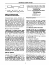
ZERO-CROSS
DETECTION
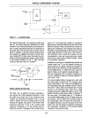
The Test 1
pin,
in
addition to being a testable
in-
put, serves two other important functions. It can
be used
as
an
input
pin
to the external event
counter, as previously mentioned, and it can be
used to detect the zero crossing
pOint
of
slow
moving
AC
signals. Execution of the STRT CNT
instruction puts the
T1
pin
in
the counter input
mode by connecting
T1
to the counter and
en-
abling the counter. Subsequent low-to-high transi-
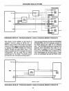
+5V
_KQ.--------,
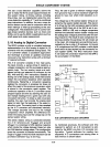
I/O PIN
PORTO
VYH
tions
on
T1
will cause the counter to increment.
Note that this operation differs from the rest of the
MCS-48 devices, which increment the counter
on
high-to-Iow transitions. This change was made
on
the 8022 to take advantage of the accuracy of the
rising edge detection
on
the zero cross circuitry.
The maximum rate at which the counter may be
incremented is once per three instruction cycles
(every
30
f./,S
when using a 3 MHz
crystaJ)-there
is
no
minimum
frequency.
In
addition to serving as a testable input
and
as the
counter input, the
T1
pin
has special circuitry to
detect when
an
AC
signal crosses its average
DC
level.
When
driven directly, this
pin
responds as a
normal digital input.
To
utilize the zero cross de-
tection mode,
an
AC
signal of approximately
1-3
VAC
pop
magnitude and a maximum frequency
of
1 kHz is coupled through
an
external capacitor
(1
f./,F)
to the
T1
pin. .
The
internal digital state is sensed as a zero until
the rising edge crosses the
DC
average level,
when it becomes a one. This is
accomplished by
the self-biasing high gain amplifier which is
includ-
ed
in
the T 1 input. This circuit biases the T 1 input
exactly at its switching point, such that a small
change will cause a digital transition to occur. This
digital transition takes place within 5 degrees of
the zero
point. The digital value of
T1
remains a
one until the falling edge of the
AC
input drops ap-
proximately 100
mV
below the switching point of
the rising edge (100
mV
below the zero
pOint,
if
the digital transition occurred exactly at the zero
point).
The
100
mV
offset is created by hysteresis
and eliminates chattering of the internal
Signal
caused by the external noise.
2-28


