8031/8051/8751
INPUT
LEVEL
AND
INTERRUPT
ENABLE
INTERRUPT REQUEST
REGISTER:
FLAG REGISTERS:
SOURCE
GLOBAL
ENABLE
ENABLE
EXTERNAL
V
INTO
-
tNT
ROST 0
INTERNAL
V
TIMER
0
EXTERNAL
V
INT1
-
INT
R08T'1
INTERNAL
V
TIMER 1
INTERNAL~
V
SERIAL
PORT
"Ft
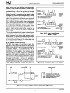
• FIVE
INTERRUPT
SOURCES
•
EACH
INTERRUPT
CAN
BE
INDIVIDUALLY
ENABLED/DISABLED
•
ENABLED
INTERRUPTS
CAN
BE
GLOBALLY
ENABLED/DISABLED
INTERRUPT
PRIORITY
REGISTER:
0-
I-
~l
POLLING
HAROWARE
~
----
SOURCE
I.D.
~
f----..
~
~
HIGH
PRIORITY
INTERRUPT
REOUEST
VECTOR
LOW
PRIORITY
INTERRUPT
REQUEST
• EACH INTERRUPT
CAN
BE ASSIGNED
TO
EITHER OF TWO PRIORITY LEVELS
•
EACH
INTERRUPT VECTORS
TO
A SEPARATE
LOCATION
IN PROGRAM MEMORY
• INTERRUPT
NESTING
TO TWO LEVELS
• EXTERNAL INTERRUPT REQUESTS
CAN
BE
PROGRAMMED
TO
BE
LEVEL~
OR
TRANSITION-ACTIVATED
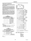
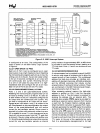
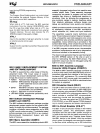
Figure
2.2.
8051
Interrupt
System
is
configured
as
an
input. The configuration of the
ports
is
shown on the
8051
Family Logic Symbol
of
Figure
2.
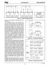
2.2.2.1 OPEN DRAIN
I/O
PINS
Each pin
of
Port 0 can be configured
as
an
open
drain output
or
as
a high impedance input. Resetting
the microcomputer programs each pin
as
an
input by
writing a one
(1)
to
the pin. If a zero
(0)
is later written
to the pin it becomes configured
as
an
output and
will continuously sink current. Re-writing the pin
to a one
(1)
will place its output driver in a high-
impedance state and configure the pin
as
an
input.
Each
I/O pin of Port 0 can sink two TTL loads.
2.2:2.2 QUASI-BIDIRECTIONAL
I/O
PINS
Ports
1,
2 and 3 are quasi-bidirectional buffers.
Resetting the microcomputer programs each pin
as
an
input by writing a one
(1)
to the pin. If a zero
(0)
is
later written to the pin it becomes configured
as
an
output and will continuously sink current. Any
pin that
is
configured
as
an
output will
be
recon-
figured
as
an input when a one
(1)
is
written to the
pin.
Simultaneous
to
this reconfiguration the output
driver
of
the quasi-bidirectional port will source
current for two.
oscillator periods. Since current
is
sourced bnly when a bit previously
written
to
a zero
(0)
is updated
to
a one
(1),
a pin programmed
as
an
input will not source current into the TTL gate that
is
driving it if the pin
is
later written with.anoth.er one
(1).
Since the quasi-bidirectional output driver sources
current
for
only two oscillator periods,
an
internal
7-4
pullup resistor
of
approximately 20K-
to
40K-ohms
is
provided to hold the external driver's loading at a
TTL high
level. Ports
1,
2 and 3 can sink/source one
TTL
load.
2.2.2:3 MICROPROCESSOR BUS
A microprocessor bus
is
provided to permit the
8051
to
solve a wide range of problems and
to
allow the
upward growth
of
user products. This multiplexed
address and data bus provides
an
interface com-
patible with standard memories, MCS-80 peripherals
and the MCS-85 memories that include on-chip
programmable I/O ports and timing functions. These
are summarized
in
the
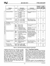
8051
Microcomputer Expan-
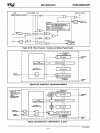
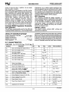
sion Cdmponents chart of Figure
2.3.
When accessing external memory the high-order
address
is
emitted on Port 2 and the low-order
address on Port
O.
The ALE signal
is
provided for
strobing the address into
an
external latch. The
program store
enable (PSEN) signal
is
provided
for
enabling
an
external memory device
to
Port 0 during
a read from the
Program Memory address space.
When the MOVX instruction
is
executed Port 3 auto-
matically generates the read (RD) Signal
for
enabling
an
External. Data Memory device to Port 0
or
gener-
ates the write
(WR)
signal for strobing the external
memory device
with
the data emitted by Port
O.
Port
o emits the address and data to the external memory
through a
push/pull
driver that can sink/source two
TTL
loads. At the end
of
the read/write bus cycle
Port 0
is automatically reprogrammed to its high
AFN-01462A-04


