8031/8051/8751
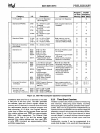
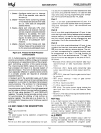
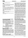
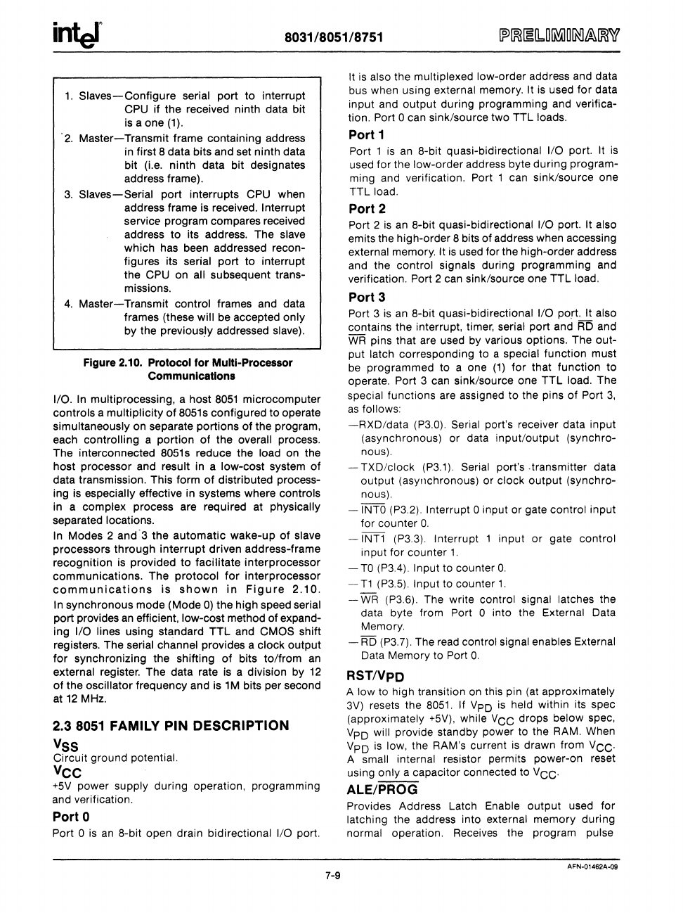
1.
Slaves-Configure
serial port to interrupt
CPU
if
the received ninth data bit
is
a one
(1).
2.
Master-Transmit frame containing address
in first 8 data bits and set ninth data
bit
(Le.
ninth data bit designates
address frame).
3.
Slaves-Serial
port interrupts CPU when
address frame is received. Interrupt
service program compares received
address to its address. The slave
which
has
been addressed recon-
figures its serial port to interrupt
the
CPU
on all subsequent trans-
missions.
4.
Master-Transmit control frames and data
frames (these
will
be
accepted only
by the previous.ly addressed slave).
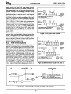
Figure
2.10.
Protocol
for
Multi-Processor
Communications
I/O.
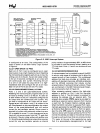
In
multiprocessing, a host
8051
microcomputer
controls a multiplicity
of
8051s
configured to operate
simultaneously on separate portions
of
the program,
each controlling a portion
of
the overall process.
The interconnected
8051s
reduce the load on the
host processor and result in a low-cost system
of
data transmission. This form
of
distributed process-
ing
is
especially effective in systems where controls
in a complex process are required at physically
separated locations.
In
Modes 2 and·3 the automatic wake-up
of
slave
processors through interrupt driven address-frame
recognition is provided to facilitate interprocessor
communications. The protocol
for
interprocessor
communications
is
shown
in
Figure
2.10.
In synchronous mode (Mode
0)
the high speed serial
port provides
an
efficient, low-cost method of expand-
ing I/O lines using standard TTL and CMOS shift
registers. The serial channel provides a clock output
for synchronizing the shifting of bits to/from
an
external register. The data rate
is
a division by
12
of
the oscillator frequency and
is
1 M bits per second
at
12
MHz.
2.3 8051 FAMILY
PIN
DESCRIPTION
VSS
Circuit ground potential.
Vee
+5V
power supply during operation, programming
and verification.
Port 0
Port 0
is
an
S-bit open drain bidirectional I/O port.
7-9
It
is
also the multiplexed low-order address and data
bus when using
external memory. It
is
used for data
input and output during programming and
verifica-
tion. Port 0 can sink/source two TTL loads.
Port 1
Port 1
is
an
S-bit quasi-bidirectional I/O port. It
is
used for the low-order address byte during program-
ming and verification. Port 1 can sink/source one
TTL load.
Port 2
Port 2
is
an
S-bit quasi-bidirectional
110
port. It also
emits the high-order 8 bits of address when accessing
external memory. It
is
used
for the high-order address
and the control signals during programming and
verification.
Port 2 can sink/source one TTL load.
Port 3
Port 3
is
an
S-bit quasi-bidirectional I/O
po.rt.
It also
contains the interrupt, timer, serial port and
RD
and
WR
pins that are used by various options. The out-
put latch corresponding to a special function must
be
programmed to a one
(1)
for that function to
operate. Port 3 can sink/source one TTL load. The
special functions are assigned to the pins of Port
3,
as
follows:
-RXD/data
(P3.0). Serial port's receiver data input
(asynchronous) or data input/output
(synchro-
nous).
- TXD/clock
(P3.1).
Serial port's. transmitter data
output (asynchronous) or clock output (synchro-
nous).
-INTO
(P3.2). Interrupt 0 input or gate control input
for counter
O.
-INT1
(P3.3). Interrupt 1 input or gate control
input for counter
1.
-
TO
(P3.4). Input to counter
O.
-
T1
(P3.5). Input to counter
1.
-
WR
(P3.6). The write control signal latches the
data byte from Port 0 into the External Data
Memory.
-
RD
(P3.7).
The
read
control signal enables External
Data Memory to Port
O.
RSTIVPD
A low to high transition
on
this pin
(at
approximately
3V)
resets the
S051.
If
VpD
is
held within its spec
(approximately
+5V).
while
VCC
drops below spec,
VpD
will provide standby power to the
RAM.
When
VpD
is
low, the RAM's current
is
drawn from
VCC·
A small internal resistor permits power-on reset
using only a capacitor connected to
VCC·
ALE/PROG
Provides Address Latch Enable output used for
latching the address into external memory during
normal operation.
Receives
the program pulse
AFN·01482A-<JS


