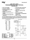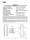
8273, 8273·4, 8273·8
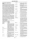
FUNCTIONAL DESCRIPTION
General
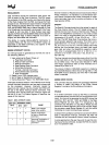
The Intel® 8273 HDLC/SDLC controller is a microcom-
puter peripheral device which supports the
International
Standards Organization (ISO) High Level Data Link
Control
(HDLC), and IBM Synchronous Data Link Control
(SDLC) communications protocols. This controller
minimizes CPU software by supporting a comprehensive
frame-level instruction set and by hardware implemen-
tation
of
the low level tasks associated with frame
assembly/disassembly and data integrity. The 8273can
be
used in either synchronous
or
asynchronous applications.
In asynchronous applications the data can
be
program-
med
to
be encoded/decoded in NRZI code. The
clock
is
derived from the
NRZI data using a digital phase locked
loop. The data transparency
is
achieved by using a zero-
bit insertion/deletion technique. The frames are automati-
cally checked
for
errors during reception by verifying the
Frame Check Sequence (FCS); the FCS
is
automatically
generated and appended before the final flag in transmit.
The 8273 recognizes and can generate flags (01111110),
Abort, Idle, and GA (EOP) characters.
The 8273 can assume either a primary
(control)
or
a
secondary (slave) role.
It can therefore be readily
implemented in
an
SDLC loop configuration
as
typified by
the IBM 3650 Retail Store System by programming the
8273 into a one-bit delay mode. In such a configuration, a
two wire pair can
be
effectively used for data transfer
between
controllers· and loop stations. The digital phase
locked loop output pin can
be
used by the
loop
station
without
the presence of
an
accurate Tx clock.
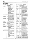
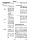
Hardware Description
The 8273 is packaged in a
40
pin DIP. The following is a
functional description
of
each pin.
Pin
Name (No.)
I/O
Description
Vee
(40)
+5V Supply
GND
(20)
Ground
RESET (4) A high signal on this pin will force
the 8273 to
an
idle state. The 8273
will remain idle until a command
is
issued by the CPU. The modem
interface
output
signals are forc-
ed
high. Reset must
be
true
for
a
minimum
of
10 TCY.
CS
(24)
The
RD
and
WR
inputs are en-
abled by the chip select input.
DB7-DBo (19-12)
I/O
The Data Bus lines are bidirec-
tional three-state lines which in-
terface with the system Data Bus.
WR
(10)
The Write signal is used to
con-
trol the transfer
of
either a com-
mand
or
data from CPU
to
the
8273.
RD
(9)
TxlNT
(2)
RxlNT
(11)
The Read signal is used
to
con-
trol the transfer
of
either a data
byte
or
a status word from the
8273 to the CPU.
o The Transmitter interrupt signal
indicates that the transmitter
logic requires service.
o The Receiver interrupt signal in-
dicates that the Receiver
logic
re-
quires service.
TxDRQ
(6)
RxRDQ
(8)
TxDACK
(5)
A1-Ao
(22-21)
TxD
(29)
TxC
(28)
RxD
(26)
RxC
(27)
32XCLi<
(25)
DPLL
(23)
FLAG DET
(1)
RTS
(35)
CTS
(30)
CD
(31)
PB1-4 (36-39)
CLK
(3)
9-69
o Requests a transfer
of
data be-
tween memory and the 8273
for
a
transmit operation.
o Requests a transfer
of
data be-
tween the 8273 and memory
for
a
receive operation.
The Transmitter DMA acknow-
ledge signal notifies the 8273 that
the
TxDMA
cycle has been
granted.
The Receiver DMA acknowledge
signal notifies the 8273 that the
RxDMA cycle has been granted.
These
two
lines are CPU Inter-
face Register Select lines.
o This line transmits the serial data
to the communication
channel.
The transmitter clock is used
to
synchronize the transmit data.
This line receives serial data from
the communication
channel.
The Receiver Clock is used
to
synchronize the receive data.
The
32X
clock is used to provide
clock recovery when an asyn-
chronous modem is used.
In
loop
configuration the
loop
station
can run
without
an
accurate 1 X
clock by using the
32X
CLK in
conjunction with the DPLL
out-
put. (This pin must be grounded
when not used).
o Digital Phase Locked Loop
out-
put can
be
tied
to
RxC
and/or
TxC when 1X clock is not avail-
able. DPLL is used with 32X CLK.
o Flag Detect signals that a flag
(01111110) has been received by
an active receiver.
o Request
to
Send signals that the
8273 is ready to transmit data.
Clear
to
Send signals that the
modem is ready
to
accept data
from the
8273.
Carrier Detect signals that the
line transmission has started and
the 8273 may begin
to
sample
data on RxD line.
General purpose
input
ports. The
logic levels on these lines can be
Read by the CPU through the
Data Bus Buffer.
o General purpose
output
ports.
The CPU can write these
output
lines through Data Bus Buffer.
A square wave
TTL
clock.


