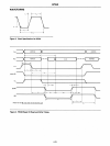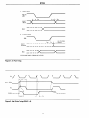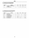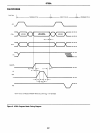
8155/8156/8155~2/8156-2
INPUT/OUTPUT
SECTION
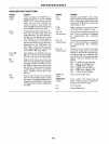
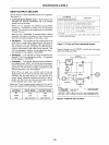
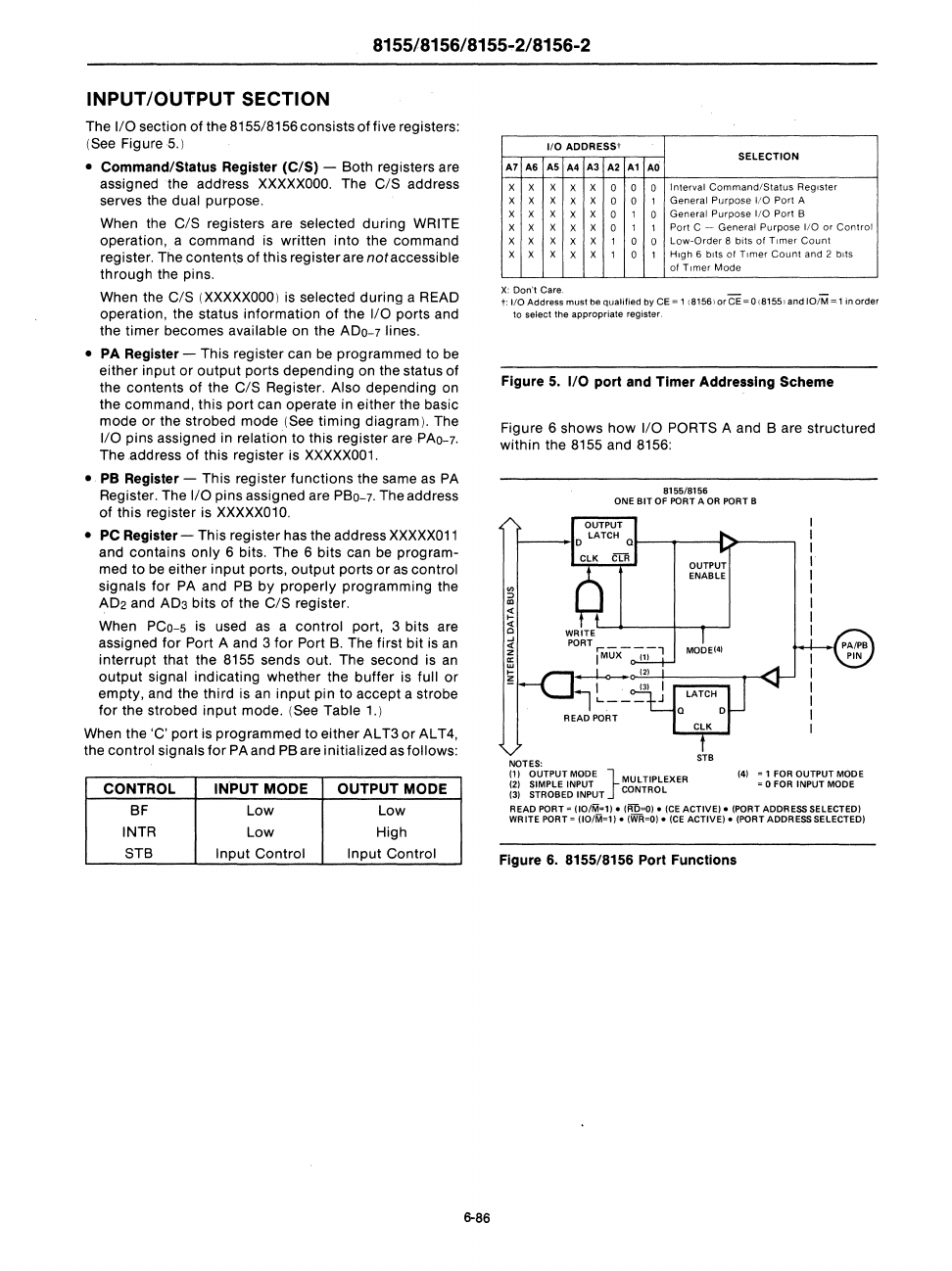
The I/O section of the 8155/8156 consists
of
five registers:
(See Figure 5.)
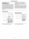
• Command/Status Register
(CIS)
- Both registers are
assigned the address
XXXXXOOO.
The CIS address
serves the dual purpose.
When the
CIS registers are selected during WRITE
operation, a command is written into the command
register. The content,s
of
this register are not accessible
through the pins.
When the CIS
(XXXXXOOO)
is
selected during a READ
operation, the status information
of
the
1/0
ports and
the timer becomes available on the ADo-7 lines.
• PA Register - This register can be programmed to
be
either input or output ports depending on the status
of
the contents of the CIS Register. Also depending on
the command, this port can operate in either the basic
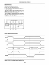
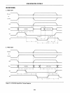
mode or the strobed mode (See timing diagram). The
I/O pins assigned in relation to this register arePAo-7.
The ,address of this register is XXXXX001.
• PB Register - This register functions the same
as
PA
Register. The
I/O
pins assigned are
PBO-7.
Theaddress
of this register is
XXXXX010.
• PC Register - This register has the address XXXXX011
and contains
only
6 bits. The 6 bits can
be
program-
med
to
be
either
input
ports,
output
ports
or
as
control
signals for
PA
and
PB
by properly programming the
AD2
and
AD3
bits of the CIS register.
When
PCO-5
is
used
as
a control port, 3 bits are
assigned for Port A and 3
for
Port
B.
The first bit
is
an
interrupt that the 8155 sends out. The second is
an
output
signal indicating whether the buffer
is
full
or
empty, and the third is
an
input
pin to accept a strobe
for the strobed
input
mode.
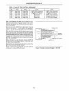
(See
Table 1.)
When the 'C' port
is
programmed to either AL T3
or
AL T4,
the control signals
for
PA
and PB are initialized
as
follows:
CONTROL
INPUT MODE
OUTPUT MODE
BF
Low
Low
INTR Low High
STB
Input
Control Input Control
6-86
1/0
ADDRESSt
SELECTION
A7 A6
AS
A4
A3 A2
A1
AD
X X X
X
X
0 0
0
Interval
Command/Status
Register
X X X
X
X
0 0 1
General
Purpose
I/O
Port
A
X X X
X
X
0
1
0
General
Purpose
1;0
PorI
B
X X
X
X X
0
1 1
Port
C -
General
Purpose
1/0
or
Control
X X X
X
X 1
a
0
low-Order
8
bits
of
Timer
Count
X X X
X
X 1
0 1
High
6
bits
of
Timer
Count
and
2
bits
of
Timer
Mode
X:
Don't
Care
__
t:
1/0
Address
must
be
qualified
by CE:= 1
181561
orCE=O
181551
and
101M"" 1 in
order
to
select the
appropriate
register
Figure 5. 1/0
port
and Timer Addressing Scheme
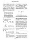
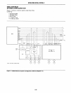
Figure 6 shows
how
1/0
PORTS A and B are structured
within the
8155 and 8156:
8155/8156
ONE BIT
OF
PORT A OR PORT B
NOTES:
(2)
SIMPLE INPUT
MULTIPLEXER
(1)
OUTPUT MODE }
(3)
STROBED INPUT CONTROL
STS
(4) '" 1 FOR OUTPUT MODE
z 0 FOR INPUT MODE
READ PORT = OO/M":o1j.
(RD=O).
(CE
ACTIVE).
(PORT ADDRESS SELECTED)
WRITE PORT =
(IO/M"'l).
(WR=O).
(CE
ACTIVE).
(PORT ADDRESS SELECTED)
Figure 6. 8155/8156 Port Functions


