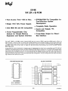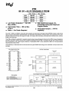
2708
FAMILY
PROGRAMMING
The
programming specifications are described in the Data Catalog PROM/ROM Programming Instructions Section.
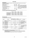
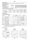
Absolute Maximum Ratings*
Temperature Under
Bias
......................
.
Storage Temperature
........................
.
Voo
With
Respect
to
VBB
......................
.
VCC
and
Vss
With Respect
to
VBB
................
.
All
Input
or'Output
Voltages With Respect
_25°C
to
+85°C
_65°C
to
+125°C
+20V
to
-0.3V
+15V
to
-0.3V
to
VBB
During Read. . . . . . . . . . . . . . . . . . . . . . .
..
+15V
to
-0.3V
CSIWE Input With Respect
to
VBB
During Programming
........................
+20V
to
-0.3V
Program I
nput
With Respect
to
VBB
..............
" +35V
to
-0
3V
Power Dissipation
...
. . . . . . . . . . . . . . . . . . . . . . . . . . . . .
..
1.5W
nco
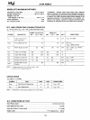
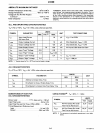
AND A.C.OPERATING CONDITIONS DURING READ
2708
2708·1
Temperature Range
0·C-70·C
0·C-70·C
Vcc Power Supply
5V±5%
5V±5%
Voo Power Supply
12V±5%
12V±5%
V
BB
Power Supply
-5V±5%
-5V:t.5%
READ OPERATION
D.C.
AND
OPERATING CHARACTERISTICS
'COMMENT
Stresses above those listed
under"
Absolute
Maximum
Ratings" may cause
permanent
damage
to
the
device.
This
is
a stress rating
only
and
functional
operation
of
the device at these·or any
other
conditions
above
those indicated in the operational sections
of
this
specification
is
not
implied. Exposure
to
absolute
maximum rating conditions for
extended
periods may
affect device reliability.
2708·6
2708L
0·C-70·C
0·C-70·C
5V±5%
5V±10%
12V±5%
12V
± 10%
-5V±5%
-5V±10%
2708.2708·1.2708,8
Limit.
2708L Limits
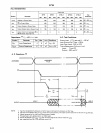
Symbol Parameter
Unit.
Te.t
Conditions
Min.
Typ.12I
Max. Min.
Typ.l2l
Max.
ILl
Address and Chip Select Input Sink 1
10
1
10
~A
V
IN
=
5.25V
or V
IN
= V
IL
Current
I
LO
Output Leakage Current
1
10
1
10
~A
VOUT
=
5.5V,
CSJWE
=
5V
100[31
Voo Supply Current
50
65
21
28
mA
Worst
Case Supply Currents[4]
IcC[3]
Vcc
Supply Current
6
10
2
4 mA
All Inputs High;
IBB[3]
V
BB
Supply Current 30
45
10
14
mA
CSWE=5V;T
A
=0'C
V
IL
Input Low Voltage
Vss
0.65
Vss
0.65
V
VIH
Input High Voltage
3.0
V
CC
+1
2.2
Vcc+
1 V
VOL
Output Low Voltage 0.45
0.4
V
10L
= 1.6mA
(2706.
2708-1,
2708-6)
10L
= 2mA (2706L)
VOH1
Output High Voltage
3.7 3.7
V
10H=
-100~A
VOH2
Output High Voltage
2.4
2.4 V
10H=
-lmA
PO
Power Dissipation
600
325
mW
T
A
=70'C
425
mW
TA=O'C
NOTES:
1.
VBB
must be applied prior to
Vcc
and Voo. V
BB
must also be the last power supply switched ofl.
2.
Typical values
are
for
TA
=
25'C
and nominal supply voltages.
3.
The
total power dissipation Is not calculated
by
summing the various currents
(1
00
• Icc, and
IBB)
multiplied by their respective vol·
tages since current paths exist between the various power supplies and Vss. The 100. Icc. and
IBB
currents should be used to deter·
mine power supply capacity only.
4.
IBB
for the 2708L Is specified in the programmed state and
is
lSmA
maximum
In
the unprogrammed state.
8-9
AFN-Qll04A-Q2


