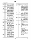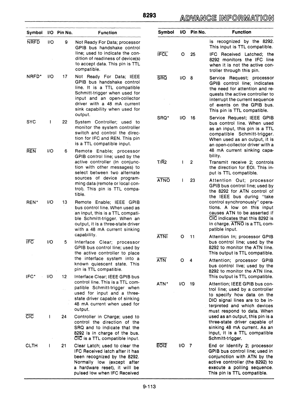
Symbol
I/O
Pin No.
Function
NRFD
1/0
9 Not Ready For Data; processor
GPIB bus handshake control
line;
used to indicate the con·
dition of readiness of device(s)
to
accept data. This pin is TTL
compatible.
NRFD'
1/0
17 Not Ready For Data;
IEEE
GPIB bus handshake control
line. It
is a TTL compatible
Schmitt·trigger
when used for
input and
an
open'collector
driver
with
a
48
mA current
sink
capability when used for
output.
SYC
22
System Controller; used to
monitor the system controller
switch and
control the direc·
tion for IFC and
REN.
This pin
is a TTL
compatible input.
REN
1/0
6 Remote Enable;
processor
GPIB control line; used
by
the
active
controller (in conjunc·
tion with other messages)
to
select between two alternate
sources of device program·
ming data (remote or local con·
trol).
This pin is TTL compa·
tible.
REN'
1/0
13
Remote Enable; IEEE GPIB
bus control line. When used as
an
input, this is a TTL compati·
ble Schmitt·trigger.
When
an
output, it is a three·state driver
with a
48
mA
current sinking
capability.
IFC I/O 5
Interface
Clear;
processor
GPIB bus control line; used
by
the active controller to place
the interface system
into
a
known quiescent state. This
pin is TTL compatible.
IFC'
I/O
12
Interface Clear; IEEEGPIB bus
control line. This is a TTL com·
patible Schmitt·trigger
when
used for input and a
three·
state driver capable of sinking
48
mA current when used for
output.
CIC
24
Controller
in
Charge; used
to
control the direction of the
SRO
and to indicate that the
8292 is in charge of the bus.
CiC
is a TTL compatible input.
CLTH
21
Clear Latch; used to clear the
IFC Received latch after it has
been recognized
by
the
8292.
Normally low (except after
a hardware reset), it will
be
pulsed low when IFC Received
8293
9-113
Symbol
I/O
Pin No.
o 25
1/0
8
SRO'
I/O
16
T/R2
2
23
o
11
o 4
ATN'
1/0
19
I/O
7
Function
is recognized by the 8292.
This input is TTL compatible.
IFC Received Latched; the
8292 monitors the
IFC line
when
it
is not the active con·
troller through this pin.
Service Request; processor
GPIB control line; indicates
the need
for
attention and
reo
quests the active controller
to
interrupt the current sequence
of events on the
GPIB bus.
This pin is TTL compatible.
Service Request;
IEEE GPIB
bus control line. When used
as
an
input, this pin is a TTL
compatible
Schmitt·trigger.
When used as
an
output,
it
is
an
open·collector driver
with
a
48
mA current sinking capa·
bility.
Transmit receive
2;
controls
the direction for
EOL
This in·
put is TTL compatible.
Attention
Out;
processor
GPIB bus control line; used
by
the
8292
for
A
TN
control of
the
IEEE bus during
"take
control synchronously" opera·
tions. A low
on
this
input
causes ATN to be asserted if
CIC indicates that this 8292 is
in charge.
ATNO is a TTL com·
patible
input.
Attention
In; processor GPIB
bus control line; used
by
the
8292
to
monitor
the ATN line.
This output is TTL compatible.
Attention;
processor
GPIB
bus control live; used
by
the
8292
to
monitor
the ATN line.
This
output
is TTL compatible.
Attention;
IEEE GPIB bus con·
trol line;
used by a controller
to specify how data
on
the
010 signal lines are to be in·
terpreted and which devices
must respond
to
data. When
used as
an
output,
this
pin is a
three·state driver capable
of
sinking
48
mA current. As
an
input,
it
is a TTL compatible
Schmitt·trigger.
End
or Identify
2;
processor
GPIB bus control line; used in
conjunction
with
ATN by the
active controller (the 8292)
to
execute a polling sequence.
This pin is TTL
compatible.


