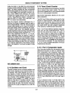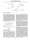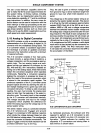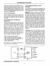
EXPANDED MCS-48 SYSTEM
ALE J
BUS
~
FLOATING
0:
FLOATING
ADDRESS
INSTRUCTION
INSTRUCTION FETCH FROM
EXTERNAL PROGRAM MEMORY
L
the conventional manner. Addresses be-
yond
2047 can be reached by executing a
program memory bank switch instruction
(SEL
MBO,
SEL MB1) followed
by
a branch
instruction (JMP
or
CALL). The bank switch
feature extends the range
of
branch
instructions beyond
their
normal 2K range
and at the same time prevents the user from
inadvertently crossing the 2K boundary.
Program
Memory
Bank
Switch
The switching of 2K program memory banks
is
accomplished
by
directly setting or resetting
the most significant bit of the program counter
(bit
11).
Bit
11
is not altered by normal incre-
menting of the program counter but is
loaded
with the contents of a special flip-flop each
time
a
JMP
or
CALL
instruction is executed.
This
special
flip-flop
is set
by
executing an
SEL
MB1
instruction and reset by SEL
MBO.
Therefore, the SEL MB instruction may be
executed at any time prior to the
actual bank
switch which occurs during the next branch
instruction encountered.
Since all twelve bits
of the program counter
including bit
(11)
are
stored
in
the stack when a Call is executed,
the user may jump to subroutines across the
2K boundary and the proper bank
will be
restored
upon return. However, the bank
switch
flipflop will not
be
altered on return.
Interrupt
Routines
Interrupts always vector the program counter
to
location 3 or 7
in
the
first
2K bank and bit
11
of the program counter is held at
"0"
during the interrupt service routine. The end
of
the service routine is signalled by the
execution of
an
RETR instruction. Interrupt
service routines
should therefore
be
contained
3·2
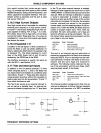
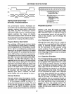
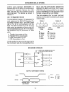
Conventional Program Counter
• Counts
DDDH
to
7FFH
• Overflow.
7FFH
to
DDDH
JMP
or
CALL Instructions trans'er oontenta
0'
Internal IIIpfiop to
A11
• Fflpflop set by SEL
MBl
• Flipflop
....
t by SEL
MBD
or
by RESET
During Interrupt
I.rvlce
routln.
A11
Is 'orced to
"0"
All
12
bits are
lav.d
In atack
PROGRAM COUNTER
entirely in the lower 2K words of program
memory. The execution of a
SEL
MBO
or SEL
MB1
instruction within an interrupt routine is
not recommended since it will not
alter
PC11
while in the routine, but will change the
internal
flip flop.
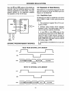
3.1.3 Restoring I/O
Port
Information
Although the lower half of Port 2 is used to
output the four most significant bits of address
during
an
external program memory fetch,
the
I/O information is still outputed during
certain portions of each machine
cycle. I/O
information is always present on Port 2 lower
at the rising edge of ALE and can
be
sampled
or latched at this time.
3.1.4 Expansion
Examples
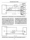
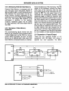
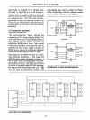
The accompanying figure shows the addition
of three
27081K X 8 EPROMs or three 2308
pin-compatible
ROM
replacements for a total
of 4K words of program memory. The BUS
port of the 8048 is connected directly to the
data output
lines of the memories. The lower
8 bits of address are latched
in
an
8212
8-bit
latch using ALE as the strobe. The lower half
of Port 2 provides the upper 4 bits of address
and since these address bits are
stable for
the duration of the program memory fetch,
they do not have to be
latched.
Two
of the
upper address bits are connected directly to
the address inputs of the memories
while the
two most significant bits are decoded to
provide the three chip
selects needed. The
PSEN output of the 8048/8748 is used to
enable the chip select lines and therefore the
memories.


