SINGLE COMPONENT SYSTEM
subroutines allowing the registers of Bank 0
used
in
the main program to be instantly
"saved" by a Bank Switch. Note that if this
second bank is not used.
locations
24-31
are
still
addressable as general purpose
RAM.
Since the two
RAM
pOinter
Registers
RO
and
R1
are
a part of the working register
array.
bank switching effectively creates two more
pointer registers
(RO'
and
R1')
which can be
used with
RO
and
R1
to easily access up to
four separate working areas
in
Ram
at one
time.
RAM
locations (8-23) also serve a dual
role
in
that they contain the program counter
stack
as
explained
in
Sec.
2.1.6.
These loca-
tions are addressed by the Stack Pointer
during subroutine calls as well as by
RAM
Pointer Registers
RO
and
R1.
If the level of
subroutine nesting is less than
8,
all
stack
registers
are
not required and can be used as
general purpose
RAM
locations. Each level of
subroutine nesting not used provides the user
with two
additional RAM locations.
2.1.4 Input/Output
The 8048 has 27 lines which can be used for
input or output functions. These
lines are
grouped as 3 ports of 8 lines each which
serve
as
either inputs, outputs or bidirectional
ORL. ANL
INTERNAL
01---41-1
BUS
-+---1D
D
FLIP
FLOP
eLK
a
WRITE_t-
__
.....
__
----'
PULSE
IN
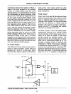
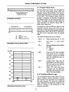
"QUASI BI DIRECTIONAL" PORT STRUCTURE
2·4
ports and 3 "test" inputs which can. alter
program sequences
when
tested by conditional
jump instructions.
Ports 1 and 2
Ports 1 and 2 are each 8 bits wide and have
identical characteristics. Data written to these
ports is statically latched and remains un-
changed until rewritten.
As
input ports these
lines are
non
latching, i.e., inputs must be
present until read by
an
input instruction.
Inputs are fully TTL compatible and outputs
will drive one standard TTL load.
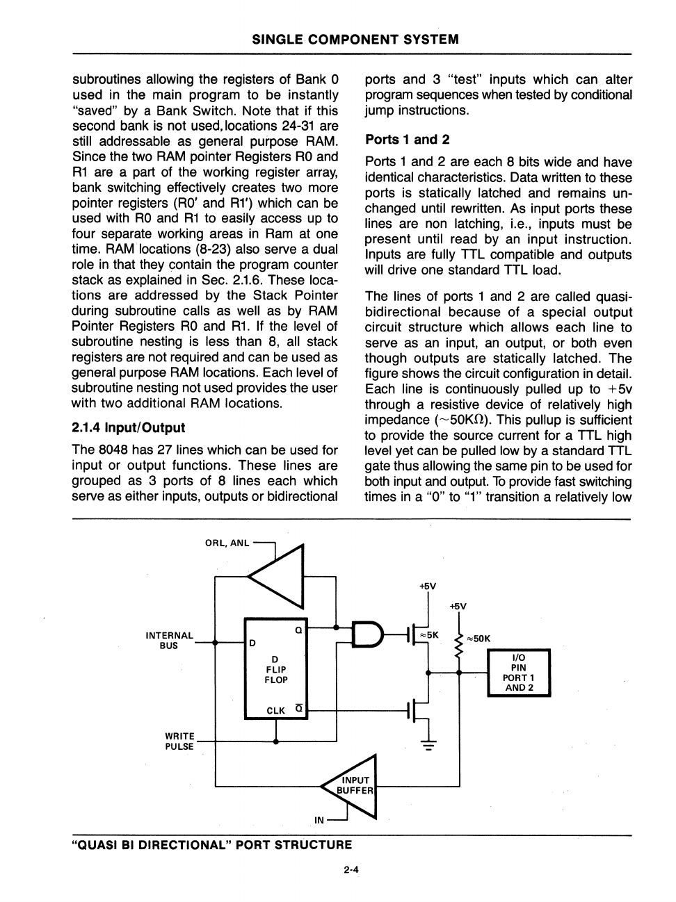
The lines of ports 1
and
2 are called quasi-
bidirectional because of a special output
circuit structure which allows each line to
serve as
an
input,
an
output, or both even
though outputs are statically latched. The
figure shows the circuit configuration
in
detail.
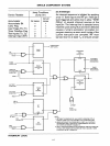
Each line is continuously pulled up to
+5v
through a resistive device of relatively high
impedance
(-50KO).
This pullup is sufficient
to provide the source current for a TTL high
level yet can be pulled low by a standard TTL
gate thus
allowing the same pin to be used for
both
input
and
output.
To
provide fast switching
times
in
a "0" to "1" transition a relatively low
+5V
+5V
"'5DK
I/O
PIN
PORT
1
AND2


