8253/8253·5
FUNCTIONAL DESCRIPTION
General
The 8253 is a programmable interval
timerlcounter
specifically designed
for
use
with
the
Intel'·
Micro-
computer
systems. Its
function
is that
of
a general
purpose,
multi-timing
element that can be treated
as
an
array
of
1/0
ports in the system software.
The 8253
solves one
of
the most common problems in any
microcomputer
system, the generation of accurate time
delays under software control. Instead
of
setting up timing
loops in systems software,
the
programmer configures the
8253
to
match his requirements, initializes one of the
counters
of
the 8253 with the desired quantity, then upon
command the 8253
will
count
out
the delay and interrupt
the CPU when it has completed its tasks.
It is easy
to
see
that
the
software overhead
is
minimal and that multiple
delays
can easily be maintained by assignment
of
priority
levels.
Other
counterltimer
functions that are non-delay in
nature but
also common
to
most microcomputers can be
implemented
with
the 8253.
• Programmable Rate Generator
• Event Counter
• Binary Rate Multiplier
• Real Time
Clock
• Digital One-Shot
• Complex
Motor
Controller
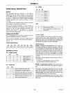
Data Bus Buffer
This 3-state, bi-directional, 8-bit buffer is used
to
interface
the 8253
to
the system data bus. Data is transmitted
or
received by the buffer upon execution
of
INput
or
OUTput
CPU instructions. The Data Bus Buffer has three basic
functions.
1.
Programming the MODES
of
the
8253.
2.
Loading the
count
registers.
3.
Reading the
count
values.
ReadIWrite Logic
The ReadlWrite
Logic
accepts inputs from the system bus
and in turn generates
control signals for overall device
operation.
It is enabled
or
disabled by CS so that no
operation can
occur
to
change the function unless
the
device has been selected
by
the system logic.
RD
(Read)
A
"low"
on this
input
informs the 8253 that the CPU is
inputting
data in the form
of
a counters value.
WR (Write)
A
"low"
on this
input
informs the 8253 that
the
CPU
is
outputting
data in the form
of
mode information
or
loading
counters.
9-7
AO,A1
These inputs are normally connected
to
the address bus.
Their
function is
to
select one
of
the
three counters
to
be
operated on and
to
address the
control
word
register
for
mode selection.
CS (Chip Select)
A
"low"
on this input enables the 8253.
No
reading
or
writing
will
occur
unless the device is selected. The CS
input
has no effect upon the actual operation
of
the
counters.
>
>.t·
.-t!
..
:.
-..;.,..;.;o.q
VIIi
-.,--".,q
.~,.",
..
"-'-~"'1
..
;Ai.'..·
.•
".
,,-"
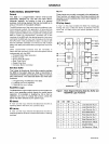
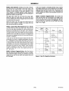
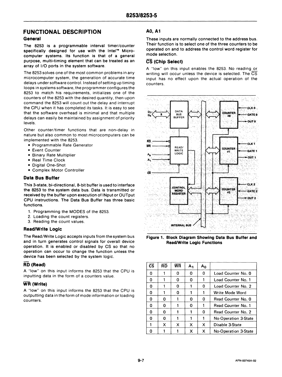
Figure
1.
Block Diagram Showing Data Bus Buffar and
RaadIWrita Logic Functions
CS
RD
WR
A,
Ao
0
1 0 0
0
Load Counter No. 0
0
1 0
0
1 Load Counter No.1
0 1 0
1
0
Load Counter
No.2
0 1 0 1 1 Write Mode Word
0 0
1
0
0
Read
Counter No. 0
0 0
1
0
1
Read
Counter
No.1
0
0
1 1 0
Read
Counter
No.2
0 0
1 1 1
No-O
peration 3-State
1
X X
X
X Disable 3-State
0
1 1
X X
No-Operation 3-State
AFN-00745A-{)2


