


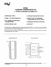

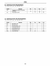
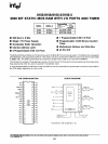
8755A
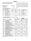
8755AFUNCTIONAL PIN DEFINITION
Symbol
ALE
(input)
ADo-7
(input/output)
AS-1o
(input)
PROG/CE1
CE2
(input)
10/M
(input)
RD
(input)
lOW
(input)
ClK
(input)
Function
When Address
latch
Enable goes
high, ADo-7,
10/M,
AS-1o,
CE2,
and
CE1
enter the address latches. The
signals (AD,
10/M,
AB-10,
CEI are
latched in at the trailing edge
of
ALE.
Bidirectional Address/Data bus. The
lower 8-bits of the PROM
or
I/O
address are applied to the bus lines
when ALE
is
high.
During
an
I/O
cycle, Port A
or
Bare
selected based on the latched value
of
ADo. If RD
or
lOR
is
low when the
latched
Chip
Enables are active, the
output
buffers present data on the
bus.
These are the high order bits
of
the
PROM address. They
do
not
affect
I/O
operations.
Chip
Enable Inputs: CE 1 is active low
and
CE2
is active high. The 8755A
can be accessed
only
when
BOTH
Chip Enables are active at the time
the ALE
signal latches them up. If
either Chip Enable
input
is
not
active,
the ADo-7 and READY
outputs
will
be in a high impedance state.
CE,
is
also used
asa
programming pin. (See
section on programming. I
If
the latched
10/M
is high when
RD
is low, the
output
data comes from
an
I/O
port. If it is
low
the
output
data
comes from the
PROM.
If
the latched Chip Enables are active
when RD goes
low, the ADo-7
output
buffers are enabled and
output
either
the selected PROM location
or
I/O
port. When both
RDand
lOR are high,
the ADo-7
output
buffers are 3-stated.
If the latched Chip Enables are active,
a
low
on lOW causes the
output
port
pOinted to
by
the latched value
of
ADo to be written with the data on
ADo-7. The state
of
10/M
is ignored.
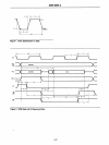
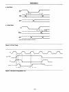
The
ClK
is used
to
force the READY
into
its high impedance state after it
has been forced
low
by
CE, low,
CE2
high, and ALE high.
6-75
Symbol
READY
(output
I
PAO-7
(input/output
1
PBO-7
(input/output
1
RESET
(inputl
lOR
(input)
Vee
Vss
Voo
Function
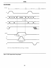
READY is a 3-state
output
controlled
by
CE2,
CEl,AlE
and
ClK.
READY
is forced
low when the
Chip
Enables
are active
during
the time ALE is high,
and remains
low
until the rising edge
of
the next
ClK.
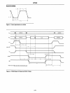
(See Figure
6.
I
These are general purpose
110
pins.
Their
input/output
direction
is
deter-
mined by the contents
of
Data Direc-
tion
Register (DDR I.
PortA
is
selected
for
write operations when the Chip
Enables are active and
lOW is
low
and a 0 was previously latched from
ADo,
AD,.
Read operation is selected
by
either
lOR
low
and active
Chip
Enables and
ADo and AD,
low,
or
10iM
high,
RD
low, active
Chip
Enables, and ADo
and
AD,
low.
This general purpose
I/O
port
is
identical to Port A except that it is
selected by a
1 latched from ADo and
a
0 from
AD1.
In normal operation,
an
input
high on
RESET causes all pins in Ports A and
B to assume
input
mode (clear DDR
register!.
When the Chip Enables are active, a
low
on lOR will
output
the selected
I/O
port onto the AD bus. lOR
low
performs the same
function
as the
combination
of
10/M
high and RD
low. When lOR is
not
used
inasystem,
lOR should be tied
to
Vce
("1"1.
+5
volt supply.
Ground
Reference.
Voo is a
programming
voltage, and
must be tied to
+5V
when the 8755A
is
being read.
For programming, a high voltage is
supplied with
Voo=
25V, typical. (See
section on programming.)