SINGLE COMPONENT SYSTEM
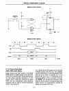
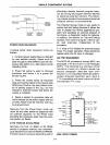
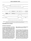
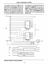
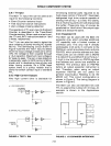
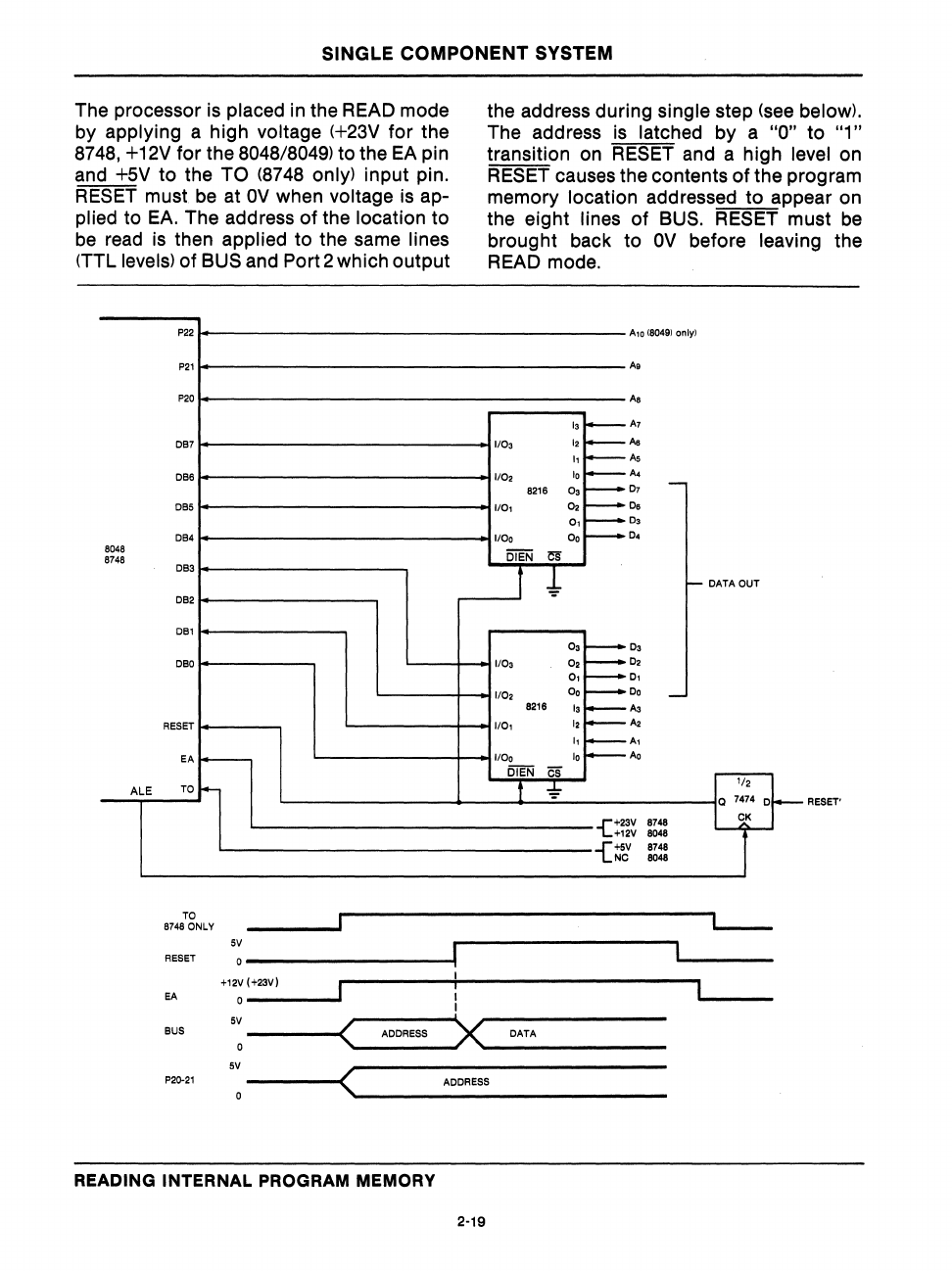
The processor is placed in the
READ
mode
by
applying a high voltage
(+23V
for the
8748,
+12V for the 8048/8049) to the
EA
pin
and +5V to the
TO
(8748
only) input pin.
RESET
must.
be
at
OV
when voltage
is
ap-
plied to
EA.
The address
of
the location to
be
read
is
then applied to the same lines
(TTL levels) of BUS and Port 2 which output
P22
P21
P20
DB7
DB8
DBS
DB4
804B
B748
DB3
DB2
OBI
DBO
RESET
EA
I---
ALE
TO
l-
TO
8748
ONLY
5V
RESET
+12V
(+23V)
EA
5V
<
BUS
ADDRESS
5V
I
i
I
I
><
the address during single step
(see
below).
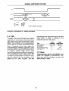
The address is latched by a "0" to "1"
transition on
RESET
and a high level on
RESET
causes the contents of the program
memory
location addressed to appear on
the eight
lines of
BUS.
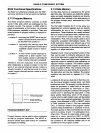
RESET must
be
brought back to
OV
before leaving the
READ
mode.
A1D
(8049)
only)
A,
Aa
I.
I----
A7
liD.
I'i--
Aa
I,
i--As
1/0,
10
I----
A4
6218
D.r-
D
,
-
110,
0,
1----00
0,1----
0
•
1100
00
r-
D
,
i5iE'N
a-
f
~
r-
DATA
OUT
O,r-
D
•
1/0.
O'r-
Do
0,1----
0,
1/0,
001----
0
0
-
8218
I.i--
A
•
1/0,
I,t---
A
,
I'I----A,
1/00
lot---Ao
i5iEN
Ci
t
~
I 1/2
Q
7474
0
-[+23V
8748
I
CK
+12V
8048
J
{+5V
8748
NC
8048
RESET'
L-
DATA
P2[J.21
<
ADDRESS
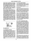
READING INTERNAL PROGRAM MEMORY
2-19


