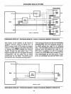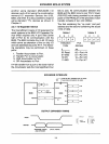
EXPANDED MCS-48 SYSTEM
MB1
PROGRAM MEMORY
SPACE
8355
(2K)
BFFH
EXTERNAL DATA
MEMORY
SPACE
MBO
400H F=====ll
8~~5
--------
300H
RESIDENT
1-::====11
8155
,...
I 10
-------
200H
(1K)
--------
100H
I
RESIDENT DATA
MEMORY
(64)
'------"
OOOH
1
________
1
SECTION
ADDRESS
PROG. MEM
OOO-BFF
DATA MEM
100-IFF
8155 PORTS
300
301
302
303
304
305
8355 PORTS 400
401
402
403
In
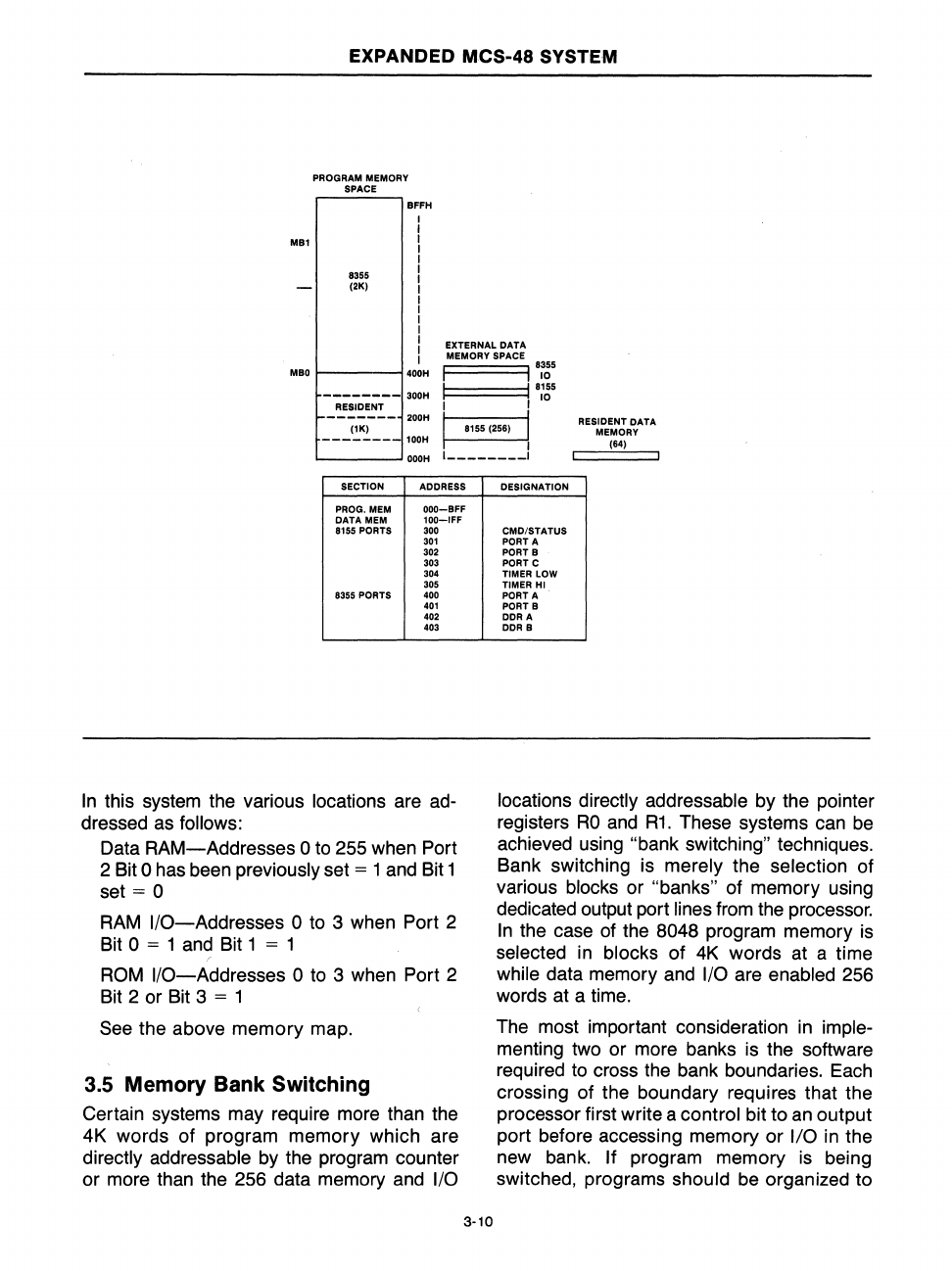
this system the various locations are
ad-
dressed as follows:
Data
RAM-Addresses
0
to
255 when Port
2 Bit
0 has been previously set = 1 and Bit 1
set = 0
RAM
I/O-Addresses
0
to
3 when Port 2
Bit
0 = 1 and Bit 1 = 1
ROM
I/O-Addresses
0
to
3 when Port 2
Bit 2 or Bit 3
= 1
See
the above memory map.
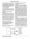
3.5 Memory Bank Switching
Certain systems may require more than the
4K words of program memory which are
directly addressable
by
the program counter
or more than the 256 data memory and
I/O
3·10
DESIGNATION
CMD/STATUS
PORTA
PORT B
PORTC
TIMER LOW
TIMER HI
PORT A
PORTB
DORA
DOR
B
locations directly addressable by the pointer
registers
RO
and
R1.
These systems
can
be
achieved using "bank switching" techniques.
Bank switching is
merely the selection of
various
blocks or "banks" of memory using
dedicated output port lines from the processor.
In
the case
of
the 8048 program memory
is
selected
in
blocks of
4K
words at a time
while data memory and I/O are enabled 256
words at a time.
The most important consideration
in
imple-
menting two or more banks is the software
required to cross the bank boundaries. Each
crossing of the boundary requires that the
processor first write a control bit to
an
output
port before accessing memory or
1/0
in
the
new bank.
If program memory
is
being
switched, programs should
be
organized to


