


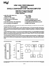
80411803118031
..
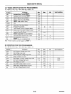
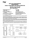
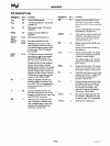
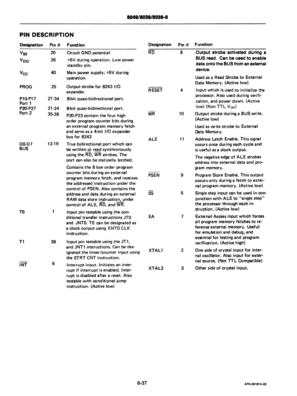
PIN DESCRIPTION
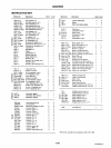
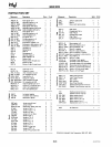
Designation
Pin
# Function
Designation
Pin
#
Function
Vss
20 Circuit GNO potential
RO
8
Output
strobe
activated
during
a
Voo
26
+5V during operation.
low
power
BUS read.
Can
be
used
to
enable
standby pin.
data
onto
the
BUS from
an
extemal
Vee
40
Main
power supply; +5V during
device.
operation.
Used as a Read Strobe
to
External
PROG
25
Output
strobe for 8243 1/0
Data Memory. (Active low)
expander.
RESET
4 Input which
is
used
to
initialize the
P10-P17
27-34
B-bit
quasi-bidirectional port.
processor_Also
used during verifi-
Port 1
cation, and power down. (Active
P2O-P27
21-24
B-bit
quasi-bidirectional port_
low)
(Non TTL
VIH)
Port 2
35-38
P2O-P23 contain
the
four high
WR
10
Output
strobe during a BUS write.
order program counter bits during
(Active
low)
an external program memory fetch
Used as write strobe
to
External
and serve as a 4-bit 1/0 expander
Data Memory.
bus for
8243
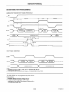
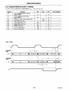
ALE
11
Address Latch Enable. This signal
00-07
12-19
True bidirectional
port
which can
occurs
once
during each cycle and
BUS
be written or read synchronously
is
useful as a clock
output.
using
the
RO,
WR
strobes. The
The negative edge
of
ALE strobes
port can
also be statically latched.
address into external data and pro-
Contains
the
8 low order program
gram memory.
counter bits during
an
external
PSEN
9
Program Store Enable. This
output
program memory fetch, and receives
the addressed instruction under
the
occurs only during a fetch
to
exter-
control
of
PSEN. Also contains
the
nal program memory. (Active low)
address and data during
an
external
55
5
Single step input can
be
used in con-
RAM
data store instruction, under
junction with ALE
to
"single
step"
control
of
ALE, RO,
and
WR.
the
processor through each in·
TO
Input pin testable using
the
con-
struc;tion. (Active low)
ditional
transfer instructions
JTO
EA
7
External Access input which forces
and
JNTO.
TO
can be designated as
all program memory fetches
to
re-
a
clock
output
using
ENTO
ClK
ference external memory. Useful
instruction.
for
emulation and debug,
and
T1
39
Input pin testable using
the
JT1,
essential
for testing
and
program
and JNT1 instructions. Can be des-
verification_ (Active high)
ignated
the
timer lcounter input using
XTAL1
2
One side
of
crystal
input
for inter-
the STRT CNT instruction.
nal oscillator. Also input for exter-
INT
6
Interrupt input. Initiates an inter-
ilalsource. (Not TTL Compatible)
rupt
if
interrupt
is
enabled. Inter-
XTAL2 3
Other side
of
crystal input_
rupt
is
disabled after a reset. Also
testable
with conditional jump
instruction. (Active
low)
6-37
AFN-00181A-Q2