


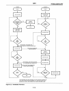

8293
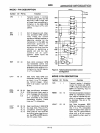
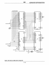
MODE 1 PIN DESCRIPTION
Symbol
I/O
Pin No.
T/R1
DAV'
D101'
D108'
3
4
I/O
24
I/O
21
I/O
25,23,
10,9,
8,7,
6,
5
I/O
22,
19,
18, 17,
16,
15,
13,
12
Function
Transmit receive
1;
controls
the direction for DAV and the
DIO
lines. If
T/R1
is high, then
all these lines are sending in·
formation
to
the IEEE GPIB
lines.
This input is TTL com·
patible.
End
of
Sequence and Atten·
tion; processor GPIB control
lines.
These
two
control
signals are ANDed together to
determine whether
all the
transceivers in the
8293
are
three·state
(push·pull)
or
open·collector. When both
signals are low (true), then the
controller
is performing a
parallel poll and the tran·
sceivers
are
all
open·
collector. These inputs are
TTL
compatible.
Data Valid; processor GPIB
bus handshake control line;
used
to
indicate the condition
(availability and validity) of in·
formation on the
DIO
signals.
It
is TTL compatible.
Data Valid;
IEEE
GPIB bus
handshake
control line. When
an
input,
it
is a TTL compati·
ble
Schmitt·trigger.
When
DAV'
is
an
output, it can sink
48
mAo
Data Input/Output; processor
GPIB bus data lines; used to
carry message and data bytes
in
a bit·parallel byte·serial
form controlled
by
the three
handshake
signals.
These
lines are TTL compatible.
Data Input/Output;
IEEE
GPIB
bus data lines. They are TTL
compatible Schmitt·triggers
when used for input and can
sink
48
mA when used for out·
put. See
ATN
and
EOI
descrip·
tion for output mode.
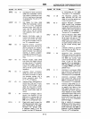
9-112
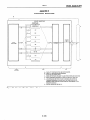
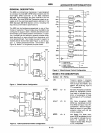
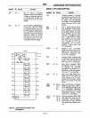
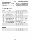
MOOE2
OPTA
OPTB
NDAi:
1--------/
1------/
NOAC'
fIm'lj
1-----+-1.
H---/NRFO'
T/ft1
~I------/.
I_---/IFC·
SYC
1-1--+---
......
-'
iIEliiH-+----H
H---/REN'
SRQ
1_+------1
I_---/SRQ·
~
~t~=+=~====~~~dl-I
ATN'
EOl2
i-+--+----t-!
~---IEOI·
Jrnm
1_+-
......
'1,
E1jj
I_+--==-:J-H
T/ft2
1_+----1+-'
iFCI
I--~_
c~~~
I=~~~...L")
Figure
5.
Talker/Listener/Controller Control
Configuration
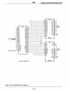
MODE 2 PIN DESCRIPTION
Symbol
I/O
Pin No.
T/R1
NDAC
I/O
10
NDAC'
I/O
18
Function
Transmit receive
1;
direction
control for NDAC and NRFD.
If
T/R1
is high, then NDAC and
NRFD
are
receiving. Input is
TTL
compatible.
Not Data Accepted; processor
GPIB bus handshake control
line;
used to indicate the con-
dition of acceptance of data
by device(s). This pin is TTL
compatible.
Not Data Accepted; IEEE
GPIB
bus handshake control
line. It
is a TTL compatible
Schmitt-trigger
when used for
input and
an
open-collector
driver with a
48
mA current
sink
capability when used for
output.