in1:ef
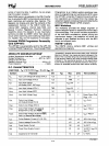
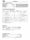
2114A FAMILY
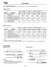
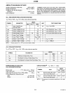
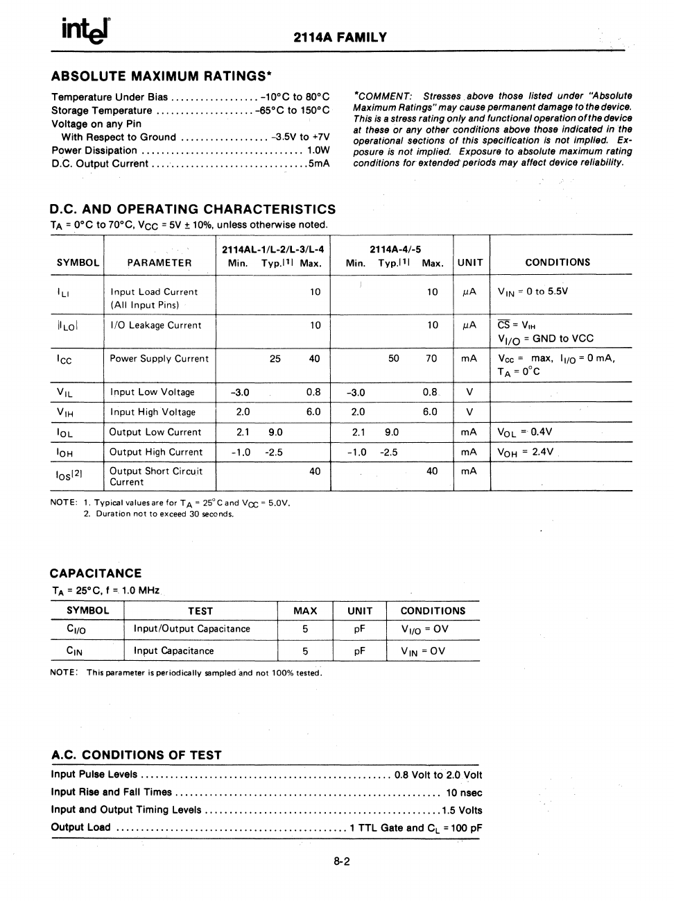
ABSOLUTE MAXIMUM
RATINGS·
Temperature
Under
Bias
..................
-lOoC
to
80°C
Storage Temperature
....................
-6SoC
to
1S0°C
Voltage
on
any Pin
With Respect
to
Ground
..................
-3.SV
to
+7V
Power Dissipation
...............................•.
1.0W
D.C.
Output
Current
................................
SmA
D.C. AND OPERATING CHARACTERISTICS
TA
= O°C
to
70°C,
Vee
=
sv
±
10%,
unless otherwise noted.
2114AL-1/L-2/L-3/L-4
SYMBOL PARAMETER
Min.
Typ.111
III
Input Load Current
(All Input
Pins)
IILOI
1/0
Leakage
Current
IcC
Power Supply Current
25
VIL
Input
Low Voltage
-3.0
VIH
Input High Voltage 2.0
10L
Output
Low Current
2.1
9.0
10H
Output High Current
-1.0
-2.5
IOsI2)
Output Short Circuit
Current
NOTE:
1.
Typical
values are
for
T A = 25
0
C
and
Vee
=
5.0V.
2.
Duration
not
to
exceed
30
seconds.
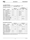
CAPACITANCE
TA
= 2SoC, f = 1.0 MHz
SYMBOL
TEST
CliO
Input/Output Capacitance
CIN
Input Capacitance
Max.
10
10
40
O.B
6.0
40
MAX
5
5
NOTE:
This
parameter
is
periodically
sampled·and
not
100%
tested.
A.C. CONDITIONS
OF
TEST
·COMMENT: Stresses. above those listed under "Absolute
Maximum Ratings" may cause permanent damage to the device.
This
is
a stress rating
only
and functional operation
ofthe
device
at these
or
any other conditions above those indicated in the
operational sections
of
this specification
is
not implied. Ex-
posure is
not
implied. Exposure to absolute maximum rating
conditions for extended· periods may affect device reliability.
2114A-4/-S
Min.
Typ.lll
Max.
UNIT
CONDITIONS
10
/lA
V
,N
~
0 to
5.SV
10
/lA
CS
~
V'H
VI/O
=
GND
to
VCC
50
70
mA
Vee
=
max,
11/0
= 0 mA,
TA
=
DoC
-3.0
O.B
V
2.0 6.0
V
2.1
9.0
mA
VOL
=
O.4V
-1.0
-2.5
mA
VOH
~
2.4V
40
mA
UNIT
CONDITIONS
pF
V'/O
~
OV
pF
VIN
=
OV
Input Pulse Levels
...................................................
0.8 Volt
to
2.0 Volt
Input
Rise and Fall Times
......................................................
10 nsec
Input
and
Output
Timing
Levels
................................................
1.5 Volts
Output
Load
...............................................
1 TTL Gate and C
L
= 100 pF
8-2


