


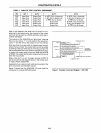

8155/8156/8155-2/8156-2
8155/8156
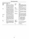
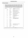
PIN
FUNCTIONS
§ymbol
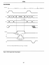
RESET
(input)
ADo-7
(input)
CE
or
CE
(input)
RD
(input)
WR
(input)
Function
Pulse provided
by
the 8085A to ini-
tialize the system (connect
to
8085A
RESET OUT). Input high on this line
resets the chip and initializes the
three
1/0 ports
to
input
mode. The
width
of
RESETpulseshouldtypically
be
two
8085A
clock
cycle times.
3-state AddresslData
lines that inter-
face with the CPU
lower 8-bit Ad-
dresslData Bus. The
8-bit
address
is
latched
into
the address latch inside
the
8155156 on the falling edge of
ALE. The address can be either for
the memory section
or
the
1/0
section
depending on the
10iiVi input. The
8-bit data is
either
written into the
chip
or
read from the chip, depending
on the
WR
or
RD
input
signal.
Chi'p Enable: On the 8155, this pin
is
CE and is ACTIVE LOW. On the 8156,
this pin is CE and is
ACTIVE HIGH.
Read
control:
Input low on this line
with the Chip
Enable active enables
and ADo-7 buffers. If 10/iVi pin is low,
the RAM
content
will be read
out
to
the AD bus. Otherwise the content
of
the selected 1/0
port
or
commandl
status registers will be read to the
AD bus.
Write
control:
Input
low
on this line
with the Chip Enable active causes
the data on the AddresslData bus to
be written to the RAM
or
1/0
ports and
commandlstatus
register depending
on
101M.
6-83
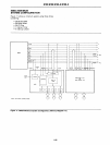
§y'mbol
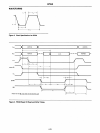
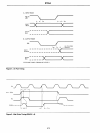
ALE
(input)
101M
(input)
PAO-7(8)
(input/output)
PBO-7(8)
(input/output)
PCo-5(6)
(input/output)
TIMER IN
(input)
TIMER
OUT
(output)
Vcc
Vss
Function
Address Latch Enable:
This
control
signal latches both the address
on
the
ADo-7 lines and the state
of
the
Chip
Enable and 101M
into
the
chip
at the
falling edge
of
ALE.
Selects memory if low and
I/O
and
commandlstatus registers
if
high.
These 8 pins are
general purpose
1/0
pins. The
inlout
direction
is selected
by
programming the
command
register.
These 8 pins are
general purpose
I/O
pins. The
inlout
direction
is selected
by programming the
command
register.
These 6 pins can
function
as
either
input
port,
output
port,
or
as
control
signals
for
PA
and
PB.
Programming
is done through the
command
reg-
ister. When
PCO-5
are used as
control
signals, they will provide the
fol-
lowing:
PCo
- A INTR (Port A Interrupt)
PC1
~
ABF (Port A Buffer Full)
PC2
- A STB (Port A Strobe)
PC3
- B INTR (Port B Interrupt)
PC4
- B BF (Port B Buffer Full)
PC5
- B STB (Port B Strobe)
Input
to
the counter-timer.
Timer output. This
output
can be
either a square wave
or
a pulse
de-
pending on the
timer
mode.
+5
volt supply.
Ground Reference.