SINGLE
COMPONENT
SYSTEM
POWER
SUPPLY 1
"""
PROCESSOR 1
~I--
INTERRUPTED
I.
I
POWER
SUPPlY---{
1 1 NORMAL
FAil
SIGNAL
~
__
I
____
POWERON
1 I 1 SEQUENCE
I I
FOllOWS
RESET i U
___
_
I
DATA SAVE
ROUTINE
EXECUTED
POWER DOWN SEQUENCE
I
ACCESS
TO
DATA
RAM
INHIBITED
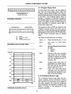
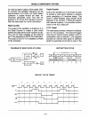
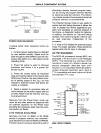
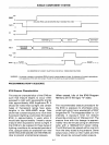
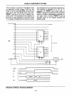
A typical power
down
sequence occurs
as
follows:
1.
Imminent
power
supply
failure
is
detected
by
user defined circuitry. Signal must
be
early enough
to
allow 8048
to
save
all
nec-
essary data before
Vee falls below normal
operating limits.
2.
Power fail signal
is
used to interrupt
processor and vector it to a power
fail
service routine.
3.
Power fail routine saves
all
important
data
and
machine status
in
the internal data
RAM
array.
Routine may also initiate trans-
fer of backup supply
to
the Voo
pin
and
indicate
to
external circuitry that power fail
routine
is
complete.
4.
Reset
is
applied
to
guarantee data will
not
be
altered
as
the power supply falls out
of
limits. Reset must
be
held
low until Vee
is
at
ground level.
Recovery
from
the Power
Down
mode
can
occur
as
any
other power-on sequence
with
an
external capacitor
on
the Reset input
providing
the
necessary
delay.
See
the previ-
ous section
on
Reset.
2.1.15
External Access Mode
Normally the first 1 K
(8048)
or
2K
(8049)
words of program memory are automati-
cally fetched from internal
ROM
or
EPROM.
The
EA
input pin however allows the userto
2-14
effectively disable internal program mem-
ory by forcing
all program memory fetches
to reference external memory. The
follow-
ing chapter explains how access to external
program memory is accomplished.
The
External Access
mode
is
very useful
in
system test
and
debug because it allows the
user
to
disable his internal applications pro-
gram
and
substitute
an
external program of
his
choice-a
diagnostic routine for instance.
In
addition, the section
on
Test
and
Debug
explains how internal program memory
can
be
read
externally, independent of the
processor.
A
"1" level
on
EA
initiates the external access
mode.
For proper operation, Reset should
be
applied while the
EA
input
is
changed.
2.2
Pin Description
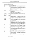
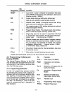
The MCS-48 processors (except
8021)
are
packaged in
40
pin Dual In-Line Packages
(DIP's). The
following
is
a summary of the
functions of each pin. Where it exists, the
second paragraph describes each pin's
function in
an
expanded MCS-48 system.
Unless otherwise specified, each input
is
TTL compatible and each output will drive
one standard TTL
load.
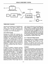
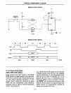
XTAL{
PORT
8
#1.
RESET
SINGLE STEP
8
PORT
.
#2
EXTERNAL
MEM.
TEST {
READ
WRITE
INTERRUPT
PROGRAM
STORE
ENABLE
ADDRESS
BUS
8
LATCH
eNABLE
8048 LOGIC SYMBOL


