1 08048/8748/8035 L
INDUSTRIAL TEMPERATURE RANGE
SINGLE COMPONENT 8·BIT MICROCOMPUTER
• 8048 Mask Programmable
ROM
• 8648 One·Time Factory Programmable EPROM
• 8748 User Programmable/Erasable EPROM
• 8035/8035L External
ROM
or
EPROM
•
- 40°C to + 85°C Operation
• 8·Bit
CPU,
ROM,
RAM,
1/0
in Single
Package
• 1 K x 8 ROMIEPROM
64
x 8
RAM
271/0
LINES
• Interchangeable
ROM
and
EPROM
Versions
• Interval TimerlEvent Counter
• Single
5V
Supply
•
2.5
fJsec
and
5.0
fJsec
Cycle Versions:
All instructions 1 or 2 Cycles
• Over
90
Instructions: 70% Single Byte
• Easily Expandable Memory and
1/0
• Compatible with 808018085 Series
Peripherals
• Single Level Interrupt
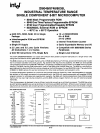
The Intel® 8048/8648/8748/8035 is a totally self·sufficient 8·bit parallel computer fabricated on a single silicon chip
using
Intel's N·channel silicon gate
MOS
process.
The
8048 contains a 1 K x 8 program memory, a
64
x 8
RAM
data memory,
271/0
lines, and
an
8·bit timerlcounter in addi·
tion
to
on·board oscillator and clock circuits. For systems that require extra capability, the 8048 can
be
expanded
using standard memories and
MCS·80™IMCS·85TM
peripherals. The 8035 is the equivalent
of
an
8048 without program
memory. The
8035L has the
RAM
power·down mode of the 8048 while the
8035
does not. The 8648 is a one·time pro·
grammable
(at the factory)
8748
which can
be
ordered as the first
25
pieces of a new 8048
ROM
order. The substitution
of
8648's for 8048's allows for very fast turnaround for initial code verification and evaluation units.
To reduce
development problems to a minimum and provide maximum flexibility, three interchangeable pin·compati·
ble
versions of this single component microcomputer exist: the 8748 with user·programmable and erasable
EPROM
program memory for prototype and preproduction systems, the 8048 with factory·programmed mask
ROM
program
memory for
low cost, high volume production, and the
8035
without program memory for use with external program
memories.
This microprocessor is designed
to
be
an
efficient controller as well as
an
arithmetic processor. The 8048 has exten·
sive
bit
handling capability as well
as
facilities for both binary and
BCD
arithmetic. Efficient use of program memory
results from
an
instruction set consisting mostly
of
single byte instructions and no instructions over 2 bytes in length.
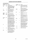
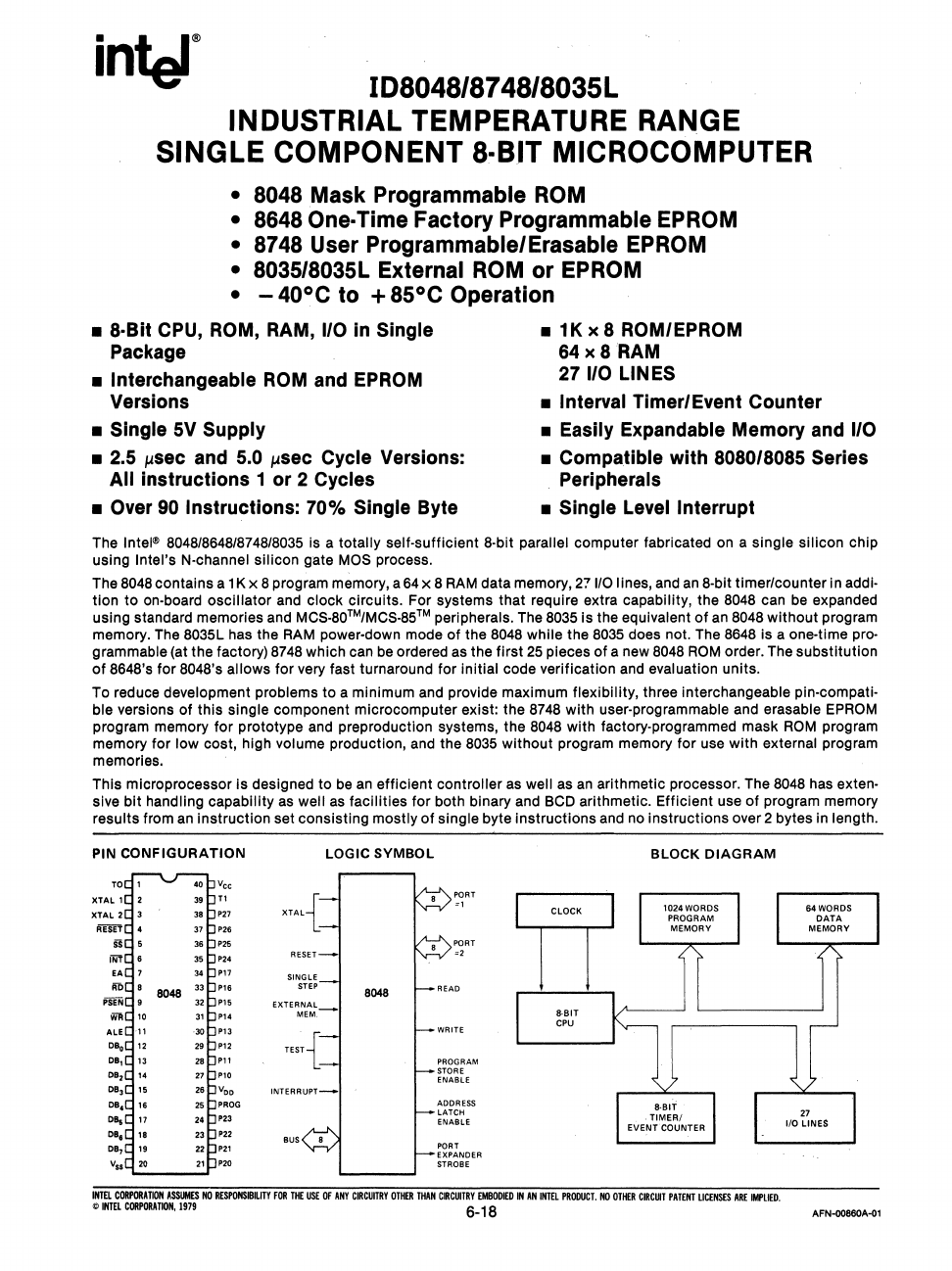
PIN
CONFIGURATION LOGIC SYMBOL
8048
PlO
ADDRESS
LATCH
ENABLE
PORT
EXPANDER
STROBE
BLOCK DIAGRAM
INTEL
CORPORATION
ASSUMES
NO
RESPONSIBILITY
FOR
THE
USE
OF
ANY
CIRCUITRY
OTHER
THAN
CIRCUITRY
EMBODIED
IN
AN
INTEL
PROOUCT.
NO
OTHER
CIRCUIT
PATENT
LlCENS(S
ARE
IMPlU
©
INTEL
CORPORATION.
1979
6-18
AFN-OOBBOA-01


