


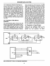
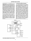

EXPANDED MCS-48 SYSTEM
fore, the
RD
and WR outputs of the 8048 are
required.
See
the following section on data
memory expansion for more detail. The sub-
sequent section on
I/O expansion explains
the operation of the
16
I/O lines.
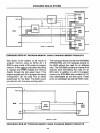
ALE
ALE
2K
X8
Pmii
iUS
WR
iOW
8048
iUS
lOR
ROM/
PROM
WITH
I/O
BUS
A/DO-7
I/O
8355/
8755
A
s
-A
10
·CS
3
TEsT I/O
INPUTS
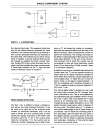
EXTERNAL PROGRAM MEMORY INTERFACE
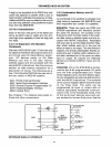
3.2
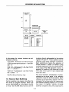
Expansion of Data Memory
Data
Memory
is expanded beyond the resi
dent
64 words by using
the
8085 type bus
feature
of
the MCS-48.
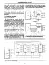
3.2.1
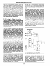
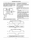
Read/Write Cycle
All
address and data is transferred over the 8
lines of BUS. A read
or
write cycle occurs as
follows:
1.
The contents of register
RO
or
R1
is out-
puted on BUS.
2.
Address Latch Enable (ALE) indicates
address is
valid. The trailing edge of ALE is
used to
latch the address externally.
3. A read (RD)
or
write (WR) pulse on the
corresponding output pins of the
8048 indi-
cates the type of data memory access
in
progress. Output data is valid at the trailing
edge of WR and input data must be
valid at
the trailing edge of
RD.
4.
Data (8-bits) is transferred in
or
out over
BUS.
READ FROM EXTERNAL
DATA
MEMORY
ALE
J
L
BUS
FLOATINcXADDRESSX
7'
>8<~
__
F_LO_A_T_IN_G
__
FLOATING
WRITE TO EXTERNAL
DATA
MEMORY
ALE
J
L
BUS
FLOATING
3·4