


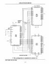
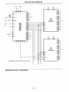
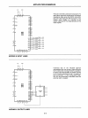
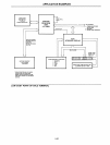
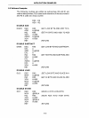
APPLICATION EXAMPLES
8049
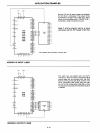
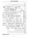
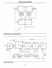
EMULATOR CIRCUIT DESCRIPTION-6 MHZ
The following is
an
explanation
of
a circuit which
emulates the operation
of
an
IntelC!>
8049
using a stan-
dard
EPROM
for program storage.
With the
8049,
software may
be
developed
by
running
external program memory, but
dOing
so requires the use
of
the bus and
P23-P20
to
access this memory.
The circuit shown may
be
used to restore the normal
functioning
of
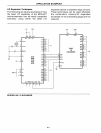
these twelve 1/0 pins. The circuit con-
sists
of
an
8039
CPU,
2716
EPROM,
two
8216
bi-
directional bus drivers, and eight other
7400
Series Low-
Power Schottky TTL packages. The whole assembly can
be built
on
a 2-3/4" x
4"
board.
A
cable coming
off
the board can
be
terminated by a
forty-pin
plug which may
be
inserted directly into the
CPU
socket intended for the
8049
In
a system undergo-
ing design or testing. Alternatively, a pattern
of
forty
pins extending
below the board can
be
used
to
plug the
board directly into the system undergoing testing,
"piggy-back" fashion. The emulator board may
be
con-
figu~ed
in
various ways so that the
40
pin plug is the
logical equivalent of
an.
8049
in every legal operating
mode.
(In
the following explanation
of
the operation
of
the circuit,
an
asterisk appearing before a signal or pin
number - as in
*PSEN
- refers to that pin on the "vir-
tual 8049"
represented by the forty-pin plug).
Since the
CPU
is Identical with the
8049
in all respects
other
than its lack
of
program memory, most
of
the pins
of
the
8039
are simply connected directly
to
the cor-
responding pins
of
the forty-pin plug. These include all
of
Port
1,
the high order bits
of
Port
2,
the test pins, etc.
Signals which are emulated with additional
!.Qgi£...!!!.·
clude the rest
of
Port
2,
DBrDBo, *PSEN, etc.
RD,
WR,
ALE, and
PSEN
are obtained from the
8039,
but are also
used by the emulation circuitry.
The
EA
input
of
the
8039
Is hard-wired high so all in-
struction fetches are made from the
2716.
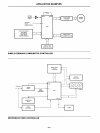
Two 74LS75
four-bit latches gated by the buffered ALE signal are
used
to
hold the lower eight bits
of
address from the
time-multiplexed data bus.
Since the Bus is being used
for fetching Instructions, data latched
to
the Bus will
be
lost on the next instruction fetch. Two 74LS174 latches
are used
to
retain the output data when a bus write is
executed. These latches are triggered
by
the trailing
edge
of
the
WR
pulse, so their outputs are glitch free.
Since logical operations
to
the bus do not generate a
WR
strobe, the
"ANL
BUS,#" and "ORL BUS,#" instruc-
tions may not
be
used, though they do function properly
with
the
other ports.
The two
8216
bi-directional bus drivers normally buffer
the latched bus contents to the
DB
pins
of
the virtual
8049. When
an
"INS A,BUS" Instruction is executed,
they buffer the input signals
on
to
the emulator data
bus.
Thus, the circuit is designed
to
use the
B1Js
for both
.Iatched output and strobed Input. If DB79DBo
of
the
8049
are to be used solely for input data, J2 and J3 may
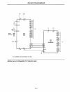
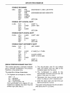
NOTE:
FOR
EMULATION
AT"11
MHZ:
1.
Substitute a
2716-1;
2.
Delete
74LS03
package
(leave
lines open). Elimination
of
74LS03
precludes
use
of
P20-P23
as
inputs.
be
changed from what is shown in the Figure, so that
DBrDBo act as high impedance inputs and the
8216s
are enabled only when the read operation Is performed.
If the bus is
to
be
used only for latched output, the
8216s can
be
omitted entirely
..
Bi-directional data transfers which require the transfer
of
address information as well as data, such as
to
and
from external data memory, require removal
of
the
8216s
and replacement with 16-pin jumper blocks on
which the
DBx
pins are connected with the respective
DOxpins.
The
lower four bits of Port 2 are also used
in
fetching in-
structions from the
2716,
in addition
to
their use as in-
put or output pins in the user's system.
In
configuring
the emulator for a particular application, the user must
dedicate each
of
these as either
an
input or output pin
and connect jumper set
J1
accordingly. Any mix of input
and output pins is
allowed. At the beginning of each in-
struction fetch, the last data written
to
P2
will
be
pre-
sent on
P23-P20
at the rising edge of ALE and will
be
latched
by
a 74LS174. The latched data may
be
con-
nected through the jumpers
to
those pins whictl will
be
used as outputs on the
8049.
Emulator pins used as in-
puts should
be
pulled above 2.0V for a logic "one". If
this is not the case, i.e.,
if
switches to Ground are to
be
read,
50K
pull up resistors should be added
to
the circuit·
on each input. They were omitted from the diagram
to
minimize input loading.
Pins which
will
be
used as inputs may
be
connected
to
the input of
an
OR
gate formed
of
inverters and open-
collector
NAND gates. The input signals will
be
relayed
directly to the
8039
and will
be
read by
an
"IN A,P2" In-
struction.But when
PSEN
is low, the NAND outputs are
forced off,
allowing the
8039
pins
to
be
used for high-
order program adressing. Open-collector 0stputs are
needed to prevent
line contention when P
EN
is not
low.
If
8243s
will
be be
used in the final system, the low order
pins of Port 2 must
be
connected directly
to
the plug.
This may
be
done by replacing the Port 2 latch with four
jumpers connecting the inputs
to
the outputs. The
NANOs should
be
removed or disabled
by
grounding the
common NAND inputs.
The
cluster of three
OR
gates Is used
to
enable the on-
board
2716
and generate the *PSEN Signal, each
of
which is a function
of
PSEN,
*EA, and the high order bit
of the program counter. Thus
*PSEN is generated, forc-
ing
an
off-board read, only when a jump has
been
made
to
Memory Bank 1 or when *EA is brought high. If this
feature is to
be
used
to
address off-board memory,
DBr
DBo
may not
be
used for normal 1/0. The
8216s
and
74LS174
must
be
replaced with jumper blocks and the
open
collector NAND gates disabled, as explained
above. The same changes are required to operate the
board in single step mode.
5-18