8292
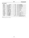
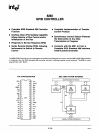
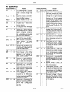
PIN DESCRIPTION
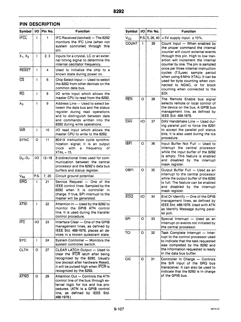
Symbol I/O Pin No. Function Symbol
1/0
Pin
No_
Function
IFCL
I
1 IFC Received (latched) - The
8292
Vee
P.S.
5,26,40
+5V
supply input. ± 10%.
monitors the IFC Line (when not
system controller)
throOgh this
pin.
COUNT
I
39
Count Input - When enabled by
the proper command the
internal
counter will count external events
X
1
,
X
2
I
2,
3
Inputs for a crystal,
LC
or
an
exter· through this pin. High to low tran-
nal timing signal to determine the sition will increment the internal
internal oscillator frequency. counter by one. The pin is sampled
RESET
I 4
Used to
initialize the chip to a
known state during power
on.
CS
I 6 Chip Select Input -
Used
to select
the
8292
from other devices on the
common data bus.
once per three
internal instruction
cycles
(7.5I'sec sample
period
when using 6 MHz
XTAL).
It can
be
used for byte counting when con'
nected to NDAC, or for
block
counting when connected to the
RD
I 8
I/O
write input which allows the
EOL
master
CPU
to
read
from the
8292.
REN
0
38
The Remote Enable
bus signal
Ao
I 9 Address Line - Used
to
select
be-
selects remote. or local control of
tween the data bus and
the status
the device on the bus. A
GPIB bus
register during
read
operations
management line,
as
defined by
and to distinguish between data
IEEE
Std.
488-1978.
and commands written into the
DAV
I/O
37
DAV
Handshake Line - Used dur-
8292
during write operations.
ing
parallel poll to force the
8291
WR
I
10
I/O
read
input which allows the
to
accept the parallel poll status
master
CPU
to write to the
8292.
bits. It is also used during the tcs
SYNC 0
11
8041
A instruction cycle synchro-
...
procedure .
nization
signal;
it
is
an
output
IBFI
0
36
Input Buffer Not Full - Used to
clock with
a
frequency of
interrupt the
central
processor
XTAL
...
15.
while the input buffer of the
8292
Do-D7
I/O
12-19 8 bidirectional lines used for com-
munication between the
central
processor and the 8292's data bus
is empty. This feature is enabled
and disabled
by
the
interrupt
mask register.
buffers and status register.
OBFI
0
35
Output Buffer Full - Used
as
an
Vss
P.S.
7,
20
Circuit ground potential.
SRO
I
21
Service Request - One of the
interrupt to the
central processor
while the output buffer of the
8292
is full. The feature can
be
enabled
IEEE
control lines. Sampled by the
8292
when it is controller in
charge. If true,
SPI
interrupt
to
the
master
will be generated.
ATNI
I
22
Attention In - Used by the
8292
to
and
disabled by the interrupt
mask register.
EOl2
I/O
34
End
Or Identify -
One
of the GPIB
management lines,
as
defined by
IEEE
Std.
488-1978.
Used with
ATN
monitor the GPIB
ATN
control
line. It
is used during the transfer
control procedure.
IFC I/O
23
Interface Clear - One of the GPIB
management lines,
as
defined
by
as
Identify Message during paral-
lel poll.
SPI
0
33
Special Interrupt - Used
as
an
interrupt on events not initiated by
the
central processor.
IEEE Std.
488-1978,
places all
de-
vices
in
a known quiescent state.
SYC
I
24
System Controller - Monitors the
TCI
0
32
Task Complete Interrupt - Inter-
rupt to the control processor used
to
indicate that the task requested
system controller switch.
was
completed by the
8292
and
CLTH
0
27
CLEAR
LATCH
Output - Used to
the information requested is ready
clear the I
FCR
latch after being
in the data bus buffer.
recognized
by
the
8292.
Usually
low (except after hardware Reset),
CIC
0
31
Controller In Charge - Controls
the
SIR
input
of
the
SRO
bus
it will
be
pulsed high when IFCR is
transceiver. It can also
be
used to
recognized by the
8292.
indicate that the
8292
is in charge
Ai1W 0
29
Attention Out - Controls the
ATN
of the GPIB bus.
control line
of
the bus through
ex-
ternal logic for
tcs
and tca pro-
cedures.
(ATN
is a GPIB control
line,
as
defined
by
IEEE
Std.
488-1978.)
9-107
00741C


