


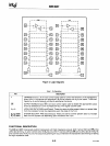
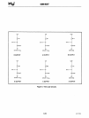
828218283
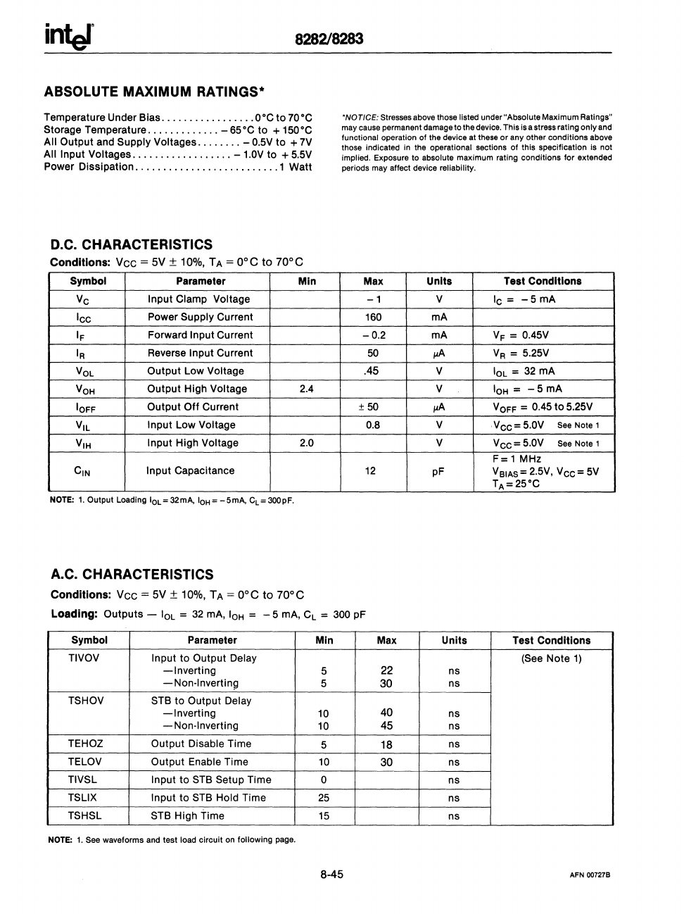
ABSOLUTE MAXIMUM RATINGS·
Temperature
Under
Bias
.................
O·C
to
70·C
Storage Temperature
.••..•.......
-65·C
to
+
150·C
All
Output
and
Supply
Voltages
........
- 0.5V
to
+ 7V
All
Input
Voltages
..................
- 1.0V
to
+ 5.5V
Power
Dissipation
.........•................
1
Watt
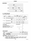
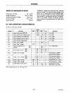
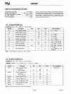
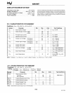
D.C. CHARACTERISTICS
Conditions:
Vee
=
5V
± 10%,
TA
=
ooe
to
70
0
e
Symbol
Parameter
Min
Vc
Input
Clamp
Voltage
Icc
Power
Supply
Current
IF
Forward
Input
Current
IR
Reverse
Input
Current
VOL
Output
Low
Voltage
V
OH
Output
High
Voltage
2.4
10FF
Output
Off
Current
V
IL
Input
Low
Voltage
V
IH
Input
High
Voltage
2.0
C
IN
Input
Capacitance
NOTE:
1.
Output
Loading
IOL=32mA,lo
H
=-5mA, C
L
=300pF.
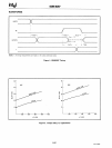
A.C. CHARACTERISTICS
Conditions:
Vee
=
5V
±
10%,
TA
=
ooe
to
70
0
e
'NOTICE:
Stresses
above
those
listed
under"AbsoluteMaxlmum
Ratings"
may
cause
permanent
damage
to
the
device.
This
is
a
stress
rating
only
and
functional operation
of
the device at these
or
any other conditions above
those
indicated
in
the
operational
sections
of
this
specification
is
not
implied.
Exposure
to
absolute
maximum
rating
conditions
for
extended
periods
may
affect
device
reliability.
Max
Units
Test
Conditions
-1
V
Ic
=
-5
rnA
160
rnA
-0.2
rnA V
F
= 0.45V
50
,..A
V
R
= 5.25V
.45
V
10L
= 32 rnA
V
10H
=
-5
rnA
± 50
,..A
VOFF
= 0.45
to
5.25V
0.8 V
.Vcc=
5.0V
See
Note
1
V
Vcc=5.0V
See
Note
1
F=
1
MHz
12
pF
V
BIAS
= 2.5V,
Vcc=
5V
T
A
=25·C
Loading:
Outputs
-
10L
= 32 rnA,
IOH
= - 5 rnA, CL = 300
pF
Symbol
Parameter
Min
Max
Units
Test
Conditions
TIVOV
Input
to
Output
Delay
(See
Note
1)
-Inverting
5
22
ns
-Non-Inverting
5
30
ns
TSHOV STB
to
Output
Delay
-Inverting
10
40
ns
-
Non·lnverting
10
45
ns
TEHOZ
Output
Disable
Time
5
18
ns
TELOV
Output
Enable
Time
10
30
ns
TIVSL
Input
to
STB
Setup
Time
0
ns
TSLIX
Input
to
STB
Hold
Time
25
ns
TSHSL
STB
High
Time
15 ns
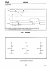
NOTE:
1.
See
waveforms
and
test
load
circuit
on
following
page.
8-45
AFN 00727B