SINGLE COMPONENT SYSTEM
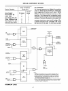
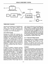
PRESCALER
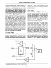
XTAL-c
15
CLEARED
ON
START TIMER
.....
----...,
START
EDGE
DETECTOR
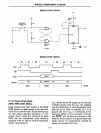
TIMER/EVENT
COUNTER
COUNTER
o
STOP
T
serviced
and
immediately
be
recognized
upon
return from the service routine. The
pending timer interrupt is reset by the
Call
to location 7
or
may
be
removed by
executing a
DIS TCNTI instruction.
As
an
Event Counter
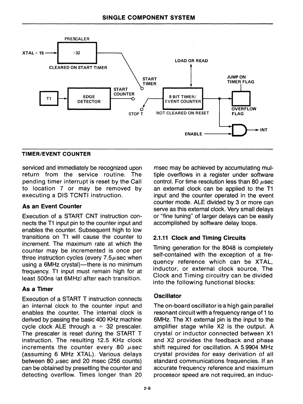
Execution of a
START
CNT instruction con-
nects the
T1
input pin to the counter input
and
enables the counter. Subsequent high to low
transitions
on
T1
will cause the counter
to
increment. The maximum rate at which the
counter may be incremented is once per
three instruction cycles (every
7.5/-tsec when
using a 6MHz
crystal)-there
is
no
minimum
frequency.
T1
input must remain high for at
least
500ns
(at
6MHz) after each transition.
As
a Timer
Execution of a
START
T instruction connects
an internal clock to the counter input and
enables the counter. The internal clock is
derived
by
passing the basic
400
KHz
machine
cycle clock
ALE
through a
-7-
32 prescaler.
The prescaler is reset during the
START T
instruction. The resulting 12.5 KHz clock
increments
the
counter
every
80 /-tsec
(assuming 6 MHz XTAL). Various delays
between
80
/-tsec
and
20 msec (256 counts)
can
be
obtained by presetting the counter
and
detecting overflow.
limes
longer than 20
2-9
LOAD OR READ
1
8 BIT
TIMER/
EVENT COUNTER
NOT
CLEARED
ON
RESET
JUMP ON
TIMER
FLAG
ENABLE
----a_~
INT
msec may
be
achieved
by
accumulating
mUl-
tiple overflows
in
a register under software
control. For time resolution less than 80
/-tsec
an
external clock can
be
applied to the
T1
input and the counter operated
in
the event
counter mode. ALE divided by 3 or more can
serve as this external clock.
Very
small delays
or
"fine tuning" of larger delays can
be
easily
accomplished by software delay loops.
2.1.11
Clock and Timing Circuits
liming
generation for the 8048 is completely
self-contained with the exception of a fre-
quency reference which can be XTAL,
inductor,
or
external
clock
source. The
Clock
and Timing
circuitry
can be divided
into the
following functional blocks:
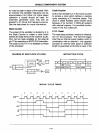
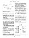
Oscillator
The on-board
oscillator
is
a high gain parallel
resonant circuit with a frequency range
of
1 to
6MHz. The
X1
external
pin
is
the input to the
amplifier stage while X2 is the output. A
crystal or
inductor
connected between
X1
and
X2
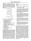
provides the feedback and phase
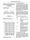
shift required for oscillation. A 5.9904 MHz
crystal provides
for
easy derivation of all
standard communications frequencies. If
an
accurate frequency reference and maximum
processor speed are not required,
an
induc-


