8251
A/S2657
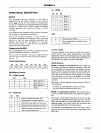
ABSOLUTE MAXIMUM RATINGS·
Ambient
Temperature Under
Bias
.........
oDe
to
70
0
e
Storage
Temperatur~
..............
-65°e
to
+150
0
e
Voltage
On
Any
Pin
With Respect
to
Ground
............
-0.5V
to +7V
Power Dissipation
.......................
1 Watt
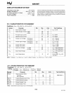
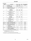
D.C. CHARACTERISTICS
T A =
OOC
to
70°C; Vee = 5.0V ±5%; GND =
OV
Symbol
Parameter
Min.
VIL
Input
Low
Voltage
-0.5
VIH
Input
High Voltage 2.2
VOL
Output
Low Voltage
VOH
Output
High Voltage 2.4
IOFL
Output
Float
Leakage
IlL
I
nput
Leakage
Icc
Power Supply Current
CAPACITANCE
T A =
2SoC;
Vee = GND =
OV
Symbol Parameter
Min. Max.
CIN
Input
Capacitance
10
CliO
I/O
Capacitance
20
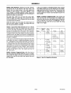
2V
<20n
1N914
8251A
1----,--+---0
OUT
C
L
"'160pF.
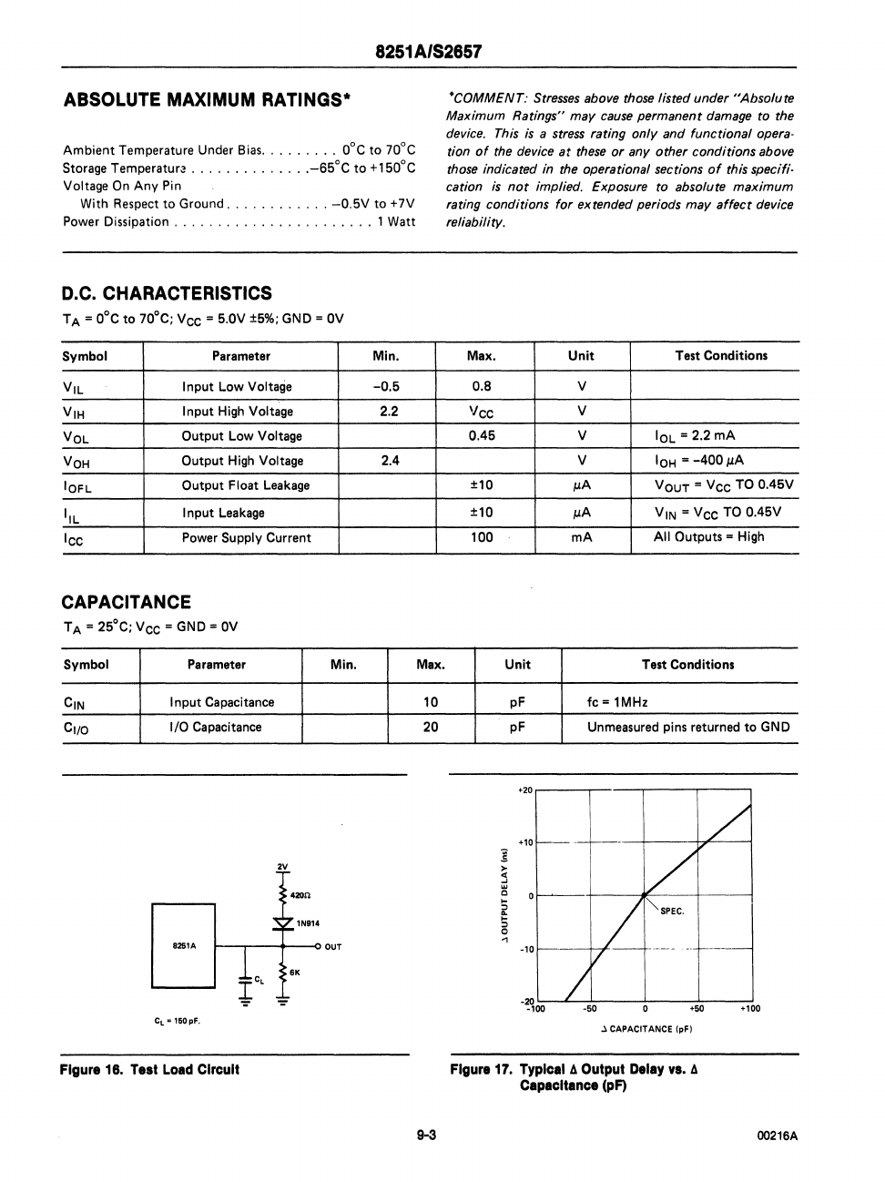
Figure 16. Test Load Circuit
9-3
'COMMENT:
Stresses
above
those
listed under
"Absolute
Maximum Ratings" may
cause
permanent damage to the
device. This
is
a
stress
rating only and functional opera-
tion
of
the device
at
these
or
any
other
conditions above
those
indicated in the operational sections
of
this specifi-
cation
is
not
implied. Exposure to absolute maximum
rating conditions
for
extended periods may
affect
device
reliability.
Max.
Unit
Test Conditions
0.8 V
'Icc
V
0.45 V
IOL
= 2.2
mA
V
IOH
=
-400
!LA
±10
!LA
VOUT =
Vee
TO O.4SV
±10
!LA
VIN =
Vee
TO 0.45V
100
mA
All
Outputs = High
Unit
Test Conditions
pF
fc
=
lMHz
pF Unmeasured pins returned
to
GND
.20,---.,-----r----,----,
+'0
~
>
~
0
...
:>
~
:>
0
..,
-'0
-20
'---'--:':----'-----='=----'
-'00
~
CAPACITANCE
(pFI
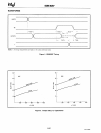
Figure 17. Typical 4 Output Delay
vs.
4
Capacitance (pF)
00216A


