


•
•
•
•
•
•
•
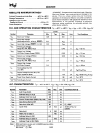
8022
SINGLE
COMPONENT
a-BIT
MICROCOMPUTER
WITH
ON-CHIP
AID
CONVERTER
8-Bit CPU,
ROM,
RAM,
1/0
in
Single 40-Pin
•
2K x 8
ROM,
64
x 8
RAM,
28
1/0
Lines
Package
•
8.38
,usec
Cycle;
All
Instructions 1
or
On-Chip 8-Bit
AID
Converter; Two Input
Cycles
Channels
8 Comparator Inputs (Port 0)
•
Instructions-8048
Subset
Zero-Cross Detection Capability
•
Interval Timer
IEvent
Counter
Single
SV
Supply (4.SV to 6.SV)
•
Clock Generated with Single Inductor
High Current Drive
Capability-2
Pins
Crystal
Two Interrupts-External and Timer
•
Easily Expanded
1/0
2
or
The
Intel@)
8022 is the newest member of the MCS-48™ family of single chip 8-bit microcomputers_ It is designed
to
satisfy the requirements of low cost, high volume applications which involve analog signals, capacitive touchpanel
keyboards, and I or large ROM space. The 8022 addresses these applications by integrating many new functions on-
chip, such as
AID
conversion, comparator inputs and zero-cross detection.
The features of the 8022
include 2K bytes of program memory (ROM), 64 bytes of data memory (RAM), 28 110 lines,
an
on-chip
AID
converter with two input channels,
an
8-bit port with comparator inputs for interfacing
to
low voltage
capacitive touchpanels
or
other non-TIL interfaces, external and timer interrupts, and zero-cross detection capabili-
ty.
In
addition,
it
contains the 8-bit interval timer I event counter, on-board oscillator and
clock
circuitry, single 5V
power
supply requirement, and easily expandable
1/0
structure common
to
all members of the MCS.-48 family.
The 8022 is designed
to
bean
efficient controller as well as
an
arithmetic processor. It has
bit
handling capability
plus facilities for both binary and
BCD
arithmetic. Efficient use of program memory results from using the MCS-48
instruction set which consists mostly of single byte instructions and has extensive conditional jump and direct table
lookup capability.
Program memory usage is further reduced via the
8022's
hardware implementation of
the
AID
converter which simplifies interfacing
to
analog signals.
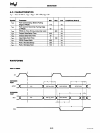
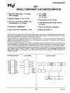
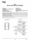
PIN CONFIGURATION
P26
P21
AVec
VAREF
ANl
AVSS
TO
P02
P03
P04
POS
PO.
P01
ALE
T1
Vss
Vee
P2S
P2'
PROG
P23
P22
P21
P20
P11
Pl.
P1S
Pl'
P13
P12
P11
Pl.
RESET
XTAL
2
XTAL
1
SUBST
XTAL
r
REseT
....
TEST
0..
TEST 1
AlD
REFERENCE
AND
...
ANl
LOGIC SYMBOL
Vee
Vss
8022
I
AID
AID SUBSTRATE
Vee
Vas
PORTO
THRESHOLD
REFERENCE
,-
___
----,
ADDRESS
LATCH
ENABLE
PORT
--EXPANDER
STROBE
6-51
BLOCK DIAGRAM
AFN-00187A-o1